

Large-Format Metrology System Debuts to Over $5 Million in Orders
BILLERICA, Mass. — (BUSINESS WIRE) — December 10, 2013 — Bruker Corporation (NASDAQ: BRKR) today announced that it has launched the ContourSP large panel metrology system, which more than doubles the measurement throughput of the high-density interconnect (HDI) substrates in multi-chip modules (MCM) over previous generation SP models used by the semiconductor packaging industry. Specifically designed to measure each layer of the printed circuit board (PCB) panels during manufacturing, the gage-capable ContourSP assures the minimum recipe development time, highest yield, maximum up-time, and lowest cost per measured panel in production. These features have already led to over $5 million in orders by several leading HDI/MCM PCB manufacturers.
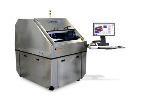
Bruker's ContourSP 3D Optical Microscope for the Printed Circuit Board Industry (Photo: Business Wire)
“Demand for Bruker’s fifth generation SP model continues to build as early adoption customers enjoy the advanced capabilities and ease of use offered by the ContourSP,” said Mark R. Munch, Ph.D., President of the Bruker MAT Group. “By doubling the throughput and adding new proprietary measurement capabilities, our customers are able to achieve maximum productivity in this era of ever smaller line widths and tighter tolerances in the PCB industry.”
“Not only is the ContourSP much faster than other systems at performing these precise measurements, but we have added a number of productivity enhancing features,” added Kent Heath, Senior Director of Marketing for Bruker’s Stylus and Optical Business. “The new Vision64® operator interface with multi-processing features multi-region analysis, automatic re-measurement, and our proprietary Dynamic Signal Segmentation (DSS) analysis, making the ContourSP the most comprehensive tool available.”
About ContourSP
Based on white light interferometry,
the ContourSP incorporates decades of packaging and panel
measurement experience to provide unprecedented speed, metrology
capability, reliability, serviceability, and manufacturing readiness for
3D critical dimension measurements in MCM and HDI PCB applications.
Bruker’s high-performance 3D optical microscopes feature Vision64
operating and analysis software, and the industry's most intuitive,
modular user interface to deliver user-level-customization capabilities
for the widest possible range of surface profiling metrology
applications. The ContourSP also utilizes Bruker’s
revolutionary gantry-based design and integrated workstation to support
up to 600x600-millimeter samples in a highly compact footprint.
About Bruker Corporation (NASDAQ:
BRKR)
Bruker is a leading
provider of high-performance scientific instruments and solutions for
molecular and materials research, as well as for diagnostics, industrial
and applied analysis. For more information, please visit
www.bruker.com.
Photos/Multimedia Gallery Available: http://www.businesswire.com/multimedia/home/20131210005117/en/
Contact:
Media Contact:
Bruker Nano Surfaces Division
Stephen
Hopkins, +1-520-741-1044 x1022
Marketing Communications
Email Contact
or
Investor
Contact:
Bruker Corporation
Joshua Young, +1-978-667-9580,
ext. 1479
Vice President, Investor Relations
Email Contact