Power considerations in sub-micron digital CMOS
2.3. From fundamental limits to practical limits of power. An architecture level approach.
Fundamental limits cannot be a basis for relative comparisons between different digital realizations. In practice we need power not only to have a reasonable probability of error but also to switch parasitic capacitances, and a certain amount of static power as a result of nonidealities of the CMOS transistors. To find practical limits of power, rules of thumb based on transistor counts were frequently used to estimate the energy consumption of a proposed digital implementation of an algorithm on chip. Unfortunately there has not been a useful relation between the energy consumption of an algorithm realized in CMOS and either its transistor count or its arithmetic complexity. The cause is the multivariable problem of power which depends on process and digital library too. In this section power at architectural level is being discussed. Without the claim of being exhaustive we try to point out the main problems.
There are four sources of power dissipation in digital CMOS circuits [11] which are summarized in the following equation:
![]() (2.6)
(2.6)
Pswitching represents the switching component of power. Pshort-circuit is due to the direct-path short circuit current Isc which arises when both the NMOS and PMOS transistors are simultaneously active. Pleakage is due to the leakage current Ileak which can arise from reverse bias diode currents and sub-threshold currents. The static power Pstatic arises in circuits that have a static biasing current between the power supplies present, for example, in class A type of logic (ECL, CML etc.). The previous equation can be rewritten in the following form:
![]() (2.7)
(2.7)
In the switching part of power, a0->1 represents the activity factor showing how many transitions per clock cycle we have. CL is the load capacitance and fs is the clock frequency. The switching power arises when energy is drawn from the power supply to charge and discharge parasitic capacitors.
A designer tries to minimize the last three terms of power when compared to the switching power. The problem can be solved by using VT management solutions which adjusts the threshold voltage of the process in order to minimize the sub-threshold currents when switching activity is low. In the following paragraphs we are considering only the switching power.
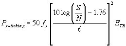
Digital algorithms can be implemented using memory elements, adders and multipliers. In DSP the switching power is a function of the number of bits B, clock frequency fs and another variable ETR that depends on the type of process and multiplier:
![]() (2.8)
(2.8)
ETR represents the energy per transition and the proportionality constant multiplied by the number of bits gives the number of operations per cycle. In [6] and [7] E. Vittoz has found relationships between power and S/N by taking a general type of multiplier and the general expression for S/N of a signal with 2B-1 discrete amplitude levels:
![]() (2.9)
(2.9)
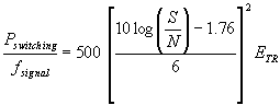
In this case, the number of operations per clock cycle was taken 50 and the power needed for multiplication is:
![]() (2.10)
(2.10)
If the number of bits are replaced in the power relation, one can find:
 (2.11)
The signal frequency fsignal and the clock frequency fS are related. Let’s assume that fS=10fsignal. In this particular case, the power per pole depends on S/N as:
 (2.12)
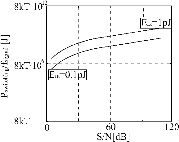
Therefore, the relationship between switching energy and signal to noise ratio S/N is logarithmic. This equation has been plotted for different ETR in fig.2.4. To be mentioned the decrease in the ETR for modern processes and therefore, this power limit is pushed down as the road-map trajectory in the modern processes shows [8]. Different multipliers have different number of operations per cycle and therefore the factor 50 in eq.(2.10) is actually dependent on the type of multiplier. Typical figures can be found in the literature [11], [12] and some of those are shown in table 1.1. Therefore, eq.(2.10) cannot be used in a general case being dependent on the type of implementation. The general equation for S/N is valid when one source of quantization errors is present. However, in a filter there are other sources of quantization errors which are introduced in the next paragraph.
|
Multiplier |
Operations/cycle |
#bits |
Reference |
|
General |
50B2 |
B*B |
Vittoz[6] |
|
General |
<40B+30B2 |
B*B |
Vittoz[7] |
|
Array |
<2.2B2 <3.4B2 |
B*B=8*8 B*B=16*16 |
|
|
Wallace Tree |
<2B2 <3.4B2 |
B*B=8*8 B*B=16*16 |
Leyten[9] |
|
Delay Balanced |
<2B2 |
B*B=24*24 |
Sakuta[10] |
Table 2.1: Operations per cycle for different multipliers
|
|
|
Fig.2.4: Energy as a function of S/N for a generic DSP |
2.3.1. Power in FIR filters.
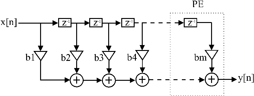
An example of a DSP algorithm is a digital filter. For the beginning consider a FIR filter with m coefficients in a one chip solution [13] as shown in fig.2.5. Here, the filter structure is composed from basic cells called processing elements PE. A processing element contains memory elements, multipliers and adders. The processing element can be distinguished within the dotted box. Given the number of states S in the filter which have to be memorized, the number of bits per word B and the number of multipliers per processing element X, we can compute the total power per DSP FIR unit PFIR:
![]()
The total power is a sum of power needed for memory Pmem, the computational power needed for adders and multipliers Pcomp and the power needed for input/output ports PI/O. The power needed for computation, Pcomp can be determined from the power per processing element PE.
|
|
|
Fig.2.5: FIR digital filter |
![]() (2.14)
(2.14)
kmult is a proportionality constant dependent on the technology and lay-out. In this particular case X=1 but it is possible to use one multiplier running mfs times faster and X=1/m with no consequences on eq. (2.14). The number of states and the number of multipliers per PE give the power needed for memory when X=S=1:
![]() (2.15)
(2.15)
In a single chip solution, the power needed for I/O operations depends on the number of bits per word B and the sampling frequency:
![]()
If the number of bits B is comparable to the number of processing elements m the power needed for memory access cannot be neglected. Moreover, for a large number of filter coefficients, the memory power will dominate over the computational power. Therefore the total power needed for FIR DSP is:
![]()
2.3.2. Power in IIR Filters
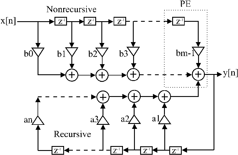
This form contains a recursive part and a non-recursive part without sharing delay elements (direct form 1) [13]. The number of processing elements PE is n+m as shown in fig.2.6. Again we have assumed memory elements as shift registers. Therefore the internal states of the filter are copied in the memory. In terms of power needed for computation there is no difference between an IIR filter and a FIR filter.
|
|
|
Fig.2.6: IIR digital filter (direct form 1) |
|
|
|
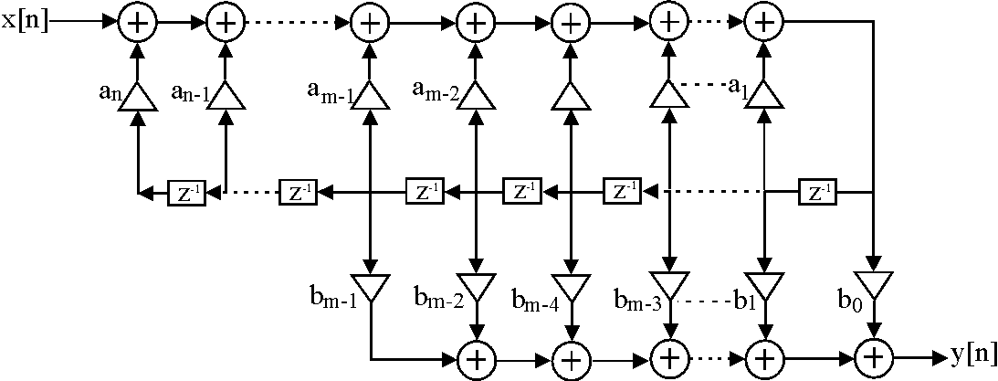
Fig.2.7: IIR digital filter (direct form 2) |
The total power will be the sum of power consumed by the recursive part and the power needed by the nonrecursive part.
![]() (2.11)
(2.11)
Given the number of processing elements m+n one can find the power needed by an direct form 1 IIR filter (IIR1) using the same considerations as in the case of a FIR filter.
![]() (2.12)
(2.12)
When the memory elements are shared, the computational power remains the same. The memory access overhead decreases by sharing some delay elements as depicted in fig.2.7 for an IIR filter direct form 2 (IIR2):
![]()
In conclusion, power needed for IIR2 DSP is smaller than the power needed for IIR1 DSP. In dedicated applications, shift registers are used as memory elements. In most applications the memory access power can be neglected when compared to computational power. Since the interconnect capacitance dominates in a shift register, the power consumed inside the registers can be neglected. Given the total capacitance at the input and at the output CTOT and the activity factor a0->1 equal for the input and for the output of the register, the power can be approximated with:
![]() (2.14 )
(2.14 )
The power for input/output operations PI/O is the power needed by the input/output registers which are clocked at the rate needed to communicate with the outside world. In a single chip solution, the dominant term, in most of the cases, remains the computational power. From now on we are referring only to this term.