Power considerations in sub-micron digital CMOS
2.6. Ways to low-power in digital
We have discussed so far power issues related to the architecture level. For every level of abstraction from fig.2.1 there are ways to reduce power which have an influence on analog functionality integrated on the same chip. In this section, we are going to point out which are the most important ways to reduce power at different levels and the consequences on analog functions [11], [12] and [16].
2.6.1. Process technology
The most effective way to reduce power at device level is to reduce the power supply voltage. This has consequences on the delay as power supply voltage approaches the threshold voltage. The problems we want to improve are:
- Increasing current drive capabilities of the devices;
- Availability of variable and multiple threshold devices for better stand-by characteristics and better matching to the analog or digital design;
- Reduced parasitic capacitances at small geometries;
- Improved interconnect technology such that interconnect scales down at the same rate as the devices;
Analog will benefit also from this except for supply voltage reduction.
2.6.2. Logic and circuit level
There are many techniques available for minimizing power at this level like:
- Clever circuit techniques to minimize device count and switching activity;
- Clever transistor sizing and VDD down scaling in the non-critical paths of the system where throughput can be reduced;
- Reducing the switching activity by logic optimization. Less switching activity will reduce the digital crosstalk;
- Choose for multi-VT logic circuits for better optimization of stand-by and dynamic power. Low VT transistors will give the best analog performance in terms of speed.
2.6.3. Power reduction at architecture level
At the architectural level of abstraction there are possible certain techniques for power reduction like:
- Architectures based on parallelism, pipelining and a combination of the two;
- Power management techniques by shutting down parts of the circuits on stand-by mode;
- The partition of memory for better power activities;
- Reduced number of busses.
2.6.4. The algorithmic level
To reduce power at the algorithm level one should be able to optimally use an algorithm such that:
- The number of operations are minimized with consequences on hardware reduction;
- Better coding for minimum switching activity by taking into account the statistics of the input signal.
2.6.5. Power at system level
At this level of abstraction a good partitioning of the system in terms of digital or analog solutions is important. Examples of methods for power reduction are:
- Integration of analog peripherals and off-chip memories on the same chip;
- Clock distribution such that system clock is a low frequency clock and internal clock generated at higher frequencies with phase locked loops.
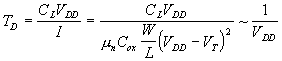
Since the average energy dissipation per cycle is proportional to CV2, where C is the load capacitance and V is the voltage swing, the obvious path to minimum power is to reduce C by scaling down minimum feature-size and especially to reduce V (see also [17]). Voltage scaling represents an efficient way to reduce power in digital. The minimum allowable value of supply voltage VDD for a static CMOS inverter was derived by R. Swanson [18] as:
![]() (2.23)
(2.23)
The condition arises from the requirement to have voltage gains larger than one. However, reducing the supply voltage down to that value has other consequences. The well known power-delay product or energy per transition, is proportional to VDD2. For a simple inverter, when VDD is down-scaled close to VTn+½ VTp½ there is a speed penalty to be paid. The simple inverter shown in fig.2.12 has a delay given by:
 ( 2.24)
|
|
|
Fig.2.12: The delay of a simple inverter |
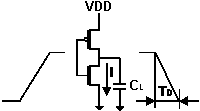
The lower the supply voltage the higher the delay. Therefore, we have to operate the circuit at the slowest possible speed. In order to maintain the throughput it is necessary to compensate for the increase of the delay by sizing-up W/L ratios of the transistors. When sizing-up the W/L of the transistors, the drain and source diffusion increases and the parasitic capacitances are increasing giving the possibility for an optimum in terms of scaling for keeping the delay constant.