Power considerations in sub-micron digital CMOS
3.2. Process tuning towards digital needs. Consequences on analog
Tuning the CMOS technology for mixed signal ICs towards digital performance and low power has numerous consequences on analog functionality. From an analog point of view the most important characteristics of a transistor are: the transconductance, the output conductance, the gate and difussion capacitances, accuracy, speed, noise and signal swing. As we will see, tuning the process towards digital performance impacts the analog functionality and the way designers would have to tackle different analog building blocks.
|
Year |
1997 |
1999 |
2001 |
2003 |
2006 |
2009 |
2012 |
|
Techno |
0.25m m |
0.18m m |
0.15m m |
0.13m m |
0.1m m |
0.07m m |
0.05m m |
|
VDD,logic[V] |
2.5...1.8 |
1.8...1.5 |
1.5...1.2 |
1.5...1.2 |
1.2...0.9 |
0.9...0.6 |
0.6...0.5 |
|
Tox,equivalent |
4..5nm |
3...4nm |
2...3nm |
2...3nm |
1.5...2nm |
1.5nm |
1nm |
|
EC [MV/cm] |
5 |
5 |
5 |
5 |
>5 |
>5 |
>5 |
Table 3.1: SIA roadmap trajectory for modern processes
Table 1 shows the roadmap trajectory predicted by Silicon Industries Association [11]. The most important factor is the gate oxide breakdown field EC. The values for VDD, logic are given from reliability consideration. For analog, the maximum supply can be derived from maximum field strength and oxide thickness. The power supply for analog functions will remain in the order of 1.5 to 2V even for technologies below one tenth of a micron and can be derived from one penlite battery with step-up converters and power management blocks. Even at this voltages designing high performance analog functions is a problem. Also it is assumed that a new replacement for SiO2 will be found and therefore the maximum field strength will increase. As far as on-chip ROM memory is becoming a fact, devices which can withstand higher voltages are available and difficult analog functions can be integrated on the same die.
3.2.1. Transconductance
The transconductance of a transistor is limited at the upper side by velocity saturation. In velocity saturation region, the transcoductance becomes constant, independent of gate length or bias:
![]() (3.1)
(3.1)
For an effective width of 1m m, the saturated transconductance has a value of about 0.25mA/V for a 0.25m m process. In many analog circuits tuning gm for process spreads by increasing the current is not effective once the velocity saturation region is trespassed. In some applications, weak inversion region can be used in order to deliver the maximum transconductance for a given current.
3.2.2. Output conductance
The output resistance is influenced by channel length modulation, static feedback and weak-avalanche effect as explained in fig.3.1. The output resistance for a given width and a given gate voltage decreases quickly at lower gate lengths. Therefore, the speed increase in deep submicron processes will be paid by a lower output resistance. It is possible for a 0.25m m CMOS process to have a unity intrinsic gain gmr0. Therefore, the device cannot be used anymore for amplification purposes. The increase of current above the velocity saturation region does not help once the transistor is velocity saturated. Enhancing the output resistance of the transistor by cascoding conflicts with low voltage requirement. Besides, the gmr0 product appears again in the expression of the output resistance after cascoding. Hence, other solutions have to be found. Techniques employing positive feedback can be considered as long as matching becomes better.
|
|
|
Fig.3.1: Output resistance and the drain current in sub- mm processes |

3.2.3. Difussion and gate capacitances
In modern technologies the gate oxide becomes thinner and subsequently Coxÿ increases. The gate-source and gate-drain capacitances scales down as the process feature size shrinks. However, the difussion capacitance goes up and because the interconnect parasitic capacitances are becoming dominant we can conclude that the load capacitance of a transistor increases.
3.2.4. Accuracy
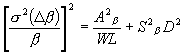
Two identical devices show a random mismatch in the parameters due to the stochastic nature of physical processes. Mismatch can be defined as the process that causes time-independent random variations in physical quantities of identically designed devices [12]. Consider the mismatch of two identical transistors which depends on the random variation of the current factor b , the threshold voltage VT0 and the body factor g . The classical theory [12], [13] applied for devices with a minimal feature size larger than 2m m makes use of the following model:
![]() (3.2)
(3.2)
![]() (3.3)
(3.3)
 (3.4)
(3.4)
The variance of the three parameters depends on the process dependent constants A and S. W and L are the gate-width and the gate length respectively and D represents the distance between the devices. The distance dependent terms can be neglected in most cases. Considering only the mismatch in VT0 shown in fig.3.2., this will improve
|
|
|
Fig.3.2: Matching in VT0 for sub- mm processes |

for deep submicron technologies due to the dependence of AVT0 on the oxide thickness dox:
![]() (3.5 )
(3.5 )
The above mentioned model is not accurate for deep submicron MOST due to narrow and short channel effects. In references [14] and [15] two other terms which account for narrow and short channels are considered in the VT0 mismatch:
![]() (3.6)
(3.6)
The second term models short channel effects and the last term models narrow channel effects. It predicts a better accuracy for devices with small gate widths and large channel lengths than the linear model.
The dependence of VT0 mismatch on the oxide thickness indicates improvement of matching when scaling down the technology towards deep sub-micron. The mismatch in the current gain factors b becomes dominant in deep sub-micron and scaling down further does not bring benefits. More about matching is discussed in the following chapters.
3.2.5. Speed
The cut-off frequency of a MOST depends on gm and the gate-source capacitance Cgs:
![]() (3.7 )
(3.7 )
This is valid in saturation and forward biasing of the transistor. Hence, modern processes have higher cut-off frequencies due to the inverse proportionality of fT with 1/L2. However this increase is being offset by the increase of difussion capacitances and the fact that interconnect cease to scale down when feature size shrinks.
3.3.6. Substrate noise
In mixed level applications another source of noise arises. It is the substrate noise or the substrate interference [16] which perturbs analog circuits due to switching in digital. Modern sub-micron technologies have low ohmic substrates and that is why substrate interferences from digital are mostly present. The effect of this source of noise is the bounce of the VSS line which can have values up to few hundreds of mV. As a consequence, the substrate bounce will reduce the dynamic range of analog circuits.
3.2.7. Signal swing
In modern processes the signal swing reduces with lowering of the power supply. Different options and scenarios are possible. The most trivial solution is multi-chip module (MCM) technology in which analog functions are implemented on a separate chip. Low VT devices are important for analog functions when voltage swing is reduced. A natural unimplanted device has a low VT and can be used for analog blocks. For digital functions, low VT devices would give an increase in the subthreshold currents. VT management solutions can be used in a twin-well process to adapt VT for the best performance. Probably the good news for analog designers is the possibility to have ROM devices which can withstand higher voltages. Therefore separate supply voltages for analog and digital is becoming a fact. The effects of signal swing on dynamic range will be extensively discussed in the next chapter.