Power considerations in sub-micron digital CMOS
3.5. From fundamental limits to practical limits. Mismatch related power
Another requirement for some of the analog signal processing circuits is related to the amount of offset they generate. Mismatch causes time independent random variations in the properties of two identically designed devices [12]. The errors produced by mismatch can be divided into systematic and random. If necessary, the systematic errors can be corrected in the design phase. To overcome the random errors, we have to use more power and intuitively it should be a connection between the two. Noise and mismatch can be treated in the same way by considering the mismatch as noise at very low frequencies. In reference [10] it is shown that Speed*Accuracy/Power ratio is fixed by technological constants meant to express the matching figures of a technology. For some applications, the impact of matching on the power required for a given speed and accuracy is even higher than the impact of noise on the power required for a given speed and dynamic range. This is simply because the variance of the noise is about two orders of magnitude lower than the variance of the offset voltages and currents. This is the case of parallel signal processing when the mismatch between the signal processing branches can influence the accuracy of the system [27], as it is the case of A/D and D/A converters [see Chapter7] and some filter applications [see Chapter 4].
- Matching in weak inversion and strong inversion
A transistor can be biased in different ways by choosing the dependent variable as current or voltage. For voltage biasing, the gate-source voltage of the devices is the same and current is the dependent variable. For current biasing, the current in the devices is the same but the voltage is the dependent variable. We can find the spread of the dependent variable from individual offset contributions. It is possible to show [10] that VT0 mismatch is dominant for nowadays sub-micron technologies:
 (3.71)
For deep sub-micron technologies VT0 mismatch will improve (fig.3.2) and it is expected that b mismatch will become dominant for L<0.18mm (see ref. [10]). If the dependent variable is current, the accuracy will increase at higher gate drive voltages. This explains why current-mode circuits should be biased deep in saturation for best accuracy. This is in contrast with voltage-mode circuits where the best accuracy is obtained in weak-inversion (
3.5.2. The Accuracy*Speed trade-off
The effect of mismatch on power consumption can be discussed from the Accuracy*Speed trade-off. The relative accuracy of a voltage or a current processing circuit is determined by the maximal input signal RMS value and the 3s value of the offset voltage or current respectively [10]:
![]() (3.72)
(3.72)
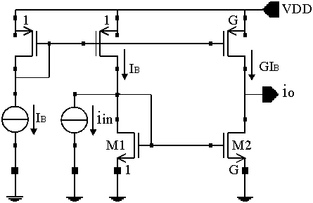
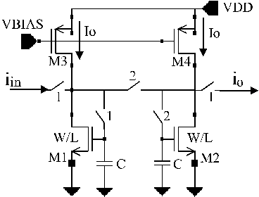
Take for example the current amplifier from fig.3.10. The offset current related to the input can be found from:
 (3.73)
For a modulation index mi, the input RMS current is miIB/Ö 2 and the relative accuracy of the stage ACC,rel:
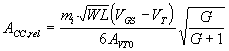 (3.74)
The power consumption of the stage is P=(G+1)IB and the Accuracy*Speed trade-off is:
 (3.75)
In conclusion, the total performance of the amplifier is dependent on technology constants, the bias point of the stage and it is independent of scaling. We want to have large gains at high speed and high accuracy at low power consumption. That is why we want to maximize the right hand side term. The extra constraint from (3.41) shows that VDD and VGS-VT cannot be chosen independently in this case. From (3.41) and (3.75) we get:
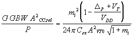 (3.76)
Eq. (3.76) shows how we can trade one specification for another. The figure of merit of the amplifier depends on physical constants and some technology dependent terms. The supply voltage and the topology of the amplifier are also involved in the trade-off. As a second order effect, by reducing the supply voltage, we have to increase the power consumption to have the same G GBW A2CC,rel product. The minimal power consumption of this stage derived from accuracy reasons is found for the ideal case when VDD>>D P+VT.
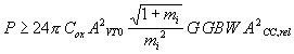 (3.77)
An important conclusion can be drawn. For a given speed, gain and accuracy, matching requirements give extra boundaries on the minimal power. This limitation is stronger than the physical limitation imposed by the effect of the thermal noise, given the levels of noise and offsets. Some of the examples considered in section 3.4. have been analyzed in reference[10] with regard to accuracy. Strong inversion or weak-inversion behavior can be treated in the same way.
In Table 3 we have presented the comparison between power consumption from dynamic range considerations versus power consumption derived from accuracy considerations. In both cases, power in voltage-mode circuits will increase faster than power for current-mode circuits when scaling down the power supply and keeping the same circuit performance. The strong inversion voltage-mode circuits from Table 3 will be biased at VGT@ 2nUT for the best performance. The same analysis can be carried out for weak-inversion operation. In the sampled data case, accuracy will be limited by charge injection. That is why results are not provided.
|
Table 3.3: Noise vs. accuracy |
Noise driven power |
Accuracy driven power |
|
|
|
|
|
|
|
|
|
|
|
|
|
|
|
|
|
|
|
|
|
|
|
________ |
|
|
|
________ |
|
|
|
________ |