Gm-C integrators for low-power and low voltage applications. A gaussian polyphase filter for mobile transceivers in 0.35
4.2. Large swing and high linearity transconductor
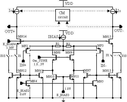
The purpose of this section is to investigate the realization of a low voltage, large swing transconductor, in a digital 0.5m CMOS technology with a constant input window and a large dynamic range over power ratio. The transconductor can be used as a Gm-C integrator for filter applications or, automatic gain control circuits (AGC). Other applications where noise and linearity are important, can be found in S -D A/D converters. This section presents a low voltage large swing transconductor in a 0.5m 3.3V CMOS digital technology [4] [5] [Electronics Letters, ECCTD] which preserves a constant input window independent of tuning. The transconductance can be digitally adjusted, in coarse steps, and continuously, in fine steps. When used as a Gm-C integrator with high Q requirements, the quality factor of the integrator can be electronically tuned. Total harmonic distortion is better than -50dB for signal amplitudes of 1.8Vpp and power consumption is 1.48mW from a 3.3V power supply.
4.2.1. Gm core principle
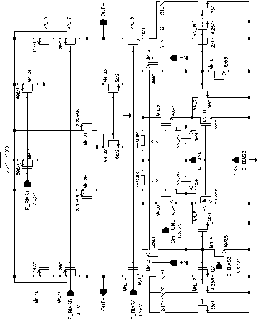
The Gm core consists of a PMOS input differential pair MP2, MP3 with degeneration resistors R1 and R2 for V to I conversion as shown in fig.4.1. The input transistors are in weak inversion for two reasons: maximal transconductance for a given current and low VGS and VDS voltages needed for large swing. MP2 (MP3) is biased under a constant current given by MN4 (MN5). The feedback loop MN6 (MN7), MN10 (MN11) and MN8 (MN9) forces a constant current in the input transistors. If the loop gain is high, the differential input voltage will be transferred to the conversion resistors R1 and R2. Any variation at the input will be sensed at the gate of MN6 (MN7) and the current of MN6 is divided between MN8 (MN9) and MN10 (MN11). The current which flows in the conversion resistors is a fraction of the current which flows in the transistor MN6. MN10 works in triode region and the value of the output conductance gives the division ratio between MN10 and MN8. In the output transistors of the transconductor, MN12 and MN13, there is a mirrored replica of the converted signal. It is to be noticed that signal currents in MN6 (MN7) are larger in comparison to the signal current which flows in the conversion resistors R1 and R2. In the conventional methods for V to I conversion [6] current is thrown away to obtain tunability.
|
|
|
Fig.4.1: Gm core diagram |
4.2.2. Transconductance tuning
Denote gm2, gm6 and gm8 the small signal transconductance of transistors MP2, MN6, MN8 and r04 the output resistance of MN4. If rDS10 represents the small signal channel resistance of MN10 in the triode region, the loop gain of the feedback loop MN6 (MN7), MN10 (MN11) and MN8 (MN9) is:
![]() (4.1)
(4.1)
Hence, the larger the output resistance of MN4 (MN5), the larger the loop gain and the higher the accuracy of the conversion. Under the assumption that r04 is infinite, we can derive by simple inspection the small signal transconductance of the converter:
![]() (4.2)
(4.2)
For a given VGS-VT, the first term in gme depends only on aspect ratio’s of MN12 and MN6. The second term comes from source degeneration and the nullor effect of the feedback loop. The last term originates from current division performed by MN8 and MN10. The transconductance can be tuned by varying the small signal output conductance of MN10 and/or by changing the aspect ratio of MN12. Tuning R1 was excluded because of a swing-tunability conflict.
a. Fine tuning
Fine tuning can be achieved by adjusting the output conductance of MN10 which depends on the effective gate-source voltage and the drain source voltage of MN10:
![]() (4.3)
(4.3)
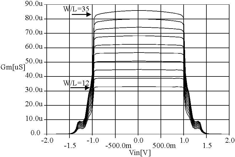
When Gm_TUNE changes, the loop keeps a constant gate source voltage for MN8 and MN9. The drain of MN10 (MN11) is pulled in the same direction as Gm_TUNE and the output conductance of MN10 will change. Now, one can see the advantage of the method: the voltage drop on the conversion resistors remains the same when Gm_TUNE varies. Therefore, for a constant VGS of MP2 and MP3 the input swing does not change with tuning. When Gm_TUNE varies from 1.8 to 3V the transconductance of the converter can be changed with about 5m A/V (10%) in a continuous way. This is shown in fig.4.2. The transconductance remains the same for an input window of 2Vpp.
b. Coarse Tuning
Process spreads require a tuning factor of about 2¸ 3 for a modern process. This cannot be achieved only from fine tuning the output conductance of MN10. Therefore, a coarse and a fine tuning are required. This can be achieved by switching transistors
|
|
|
Fig.4.2: Gm fine tuning |

with different aspect ratios at the output, for a coarse interval, and fine tuning rDS10 to get transconductances within the coarse interval as shown in fig.4.9. In this way, the transconductance can be tuned between 30m A/V and 85m A/V, in ten coarse steps, with a grid of 5m A/V for fine tuning. The smallest transistor has an aspect ratio of 12/1 and the largest transistor has an aspect ratio of 35/1. Accordingly, the transconductance varies in coarse steps from 30m A/V to 85m A/V as illustrated in fig.4.3.
|
|
|
Fig.4.3: Gm coarse tuning for different aspect ratios of MN12(13) |
4.2.3. Common-mode circuit
The common-mode circuit consists of transistors MP20, MP21, MN22, MN23 and MP24 (fig.4.9). The common-mode output voltage is sensed by MP20 and MP21 and their output signals are added up in the drain of MN22. A current mirror with active load provides common-mode feedback to the gates of MP18 and MP19. The common-mode DC voltage is thus VDD-VSG20. In our case, the common-mode at the output is 1.5V. For input-output compatibility, the input common mode voltage has been set to 1.5V. The differential output swing is limited by the input range of MP20 and MP21. This is about 1.9Vpp for current values of VGS20 and VGS21. The GBW of the common-mode amplifier is larger than the GBW of the differential amplifier in order to ensure stability for all frequencies of interest up to the GBW of differential amplifier. This condition is satisfied if gm20 is chosen larger than gme of the voltage to current converter taking into account the same load capacitance for the two amplifiers.
4.2.4. Linearity of conversion
In the voltage to current conversion the main sources of non-linearity are the current division and channel length modulation of the output transistors. The input transistor is biased with a constant current and will not give an important contribution on distortion. The THD has been simulated for different tuning conditions. In fig.4.4 the amplitude of the input signal changes from 1Vpp to 2Vpp when Gm_TUNE is zero. Under coarse tuning, at maximum Gm, in the worst case, the THD of the converter is -47dB and below -50dB for amplitudes lower than 1.86Vpp. The harmonic distortion is dominated by odd harmonics due to differential approach.
|
|
|
Fig.4.4: THD for Gm_TUNE=0 |

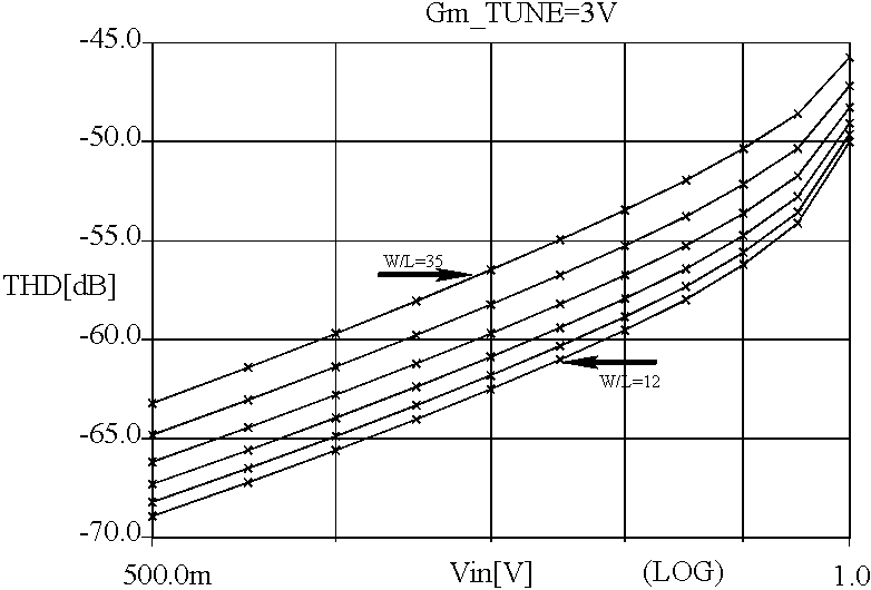
When Gm_TUNE becomes 3V, at maximum tuning, the non-linearity due to current division increases and at maximum tuning and maximum signal amplitudes THD approaches -46dB as shown in fig.4.5. This can be explained in a simple way by using the current triangle method [7]. For Gm_TUNE=0, the current division is inherently linear, independent of the working region of MN8 (MN10) and MN9 (MN11). When Gm_TUNE is larger than zero, the voltage difference between the gates of MN8 and MN10 gives extra distortion terms in the current division.
4.2.5. AC response and Q-tuning
If the transconductor is used as a Gm-C integrator, the frequency response and the phase response are important for determining the quality factor of the integrator. It is expected that using negative feedback, we get extra poles and extra phase shift at
|
|
|
Fig.4.5: THD for Gm_TUNE=3V |
GBW frequency caused by them. A simple analysis reveals the existence of a low frequency pole at GBW/AOL and a zero at:
![]() (4.4)
(4.4)
and two high frequency poles. In (4.4) Cgs8 denotes the gate-source capacitance of MN8. The condition to have two real poles can be formulated in terms of output resistance of the current source MN4.
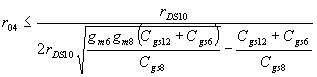 (4.5)
(4.5)
There is a trade-off between a high output resistance r04 needed for large loop gain and a relative low output resistance to avoid peaking of the loop. An optimal value for r04 to provide sufficient loop gain is in the order of a few MW . The Gm-C integrator has a GBW of 1MHz. In fig.4.6, simulations show an open loop gain of 70dB. This is sufficient for most applications. In order to make the phase close to 90° for all possible situations given by process spreads, in high Q applications Q tuning is required. However, this is a disadvantage we have to pay for linearity. The quality factor of the integrator can be tuned by using the non-linear capacitance from the gate to the substrate of a MOS transistor. In fig.4.8 Q_TUNE controls the gate-substrate capacitances of transistors MN25 and MN26. This adjustment does not interfere with Gm tuning.
4.2.6. Noise properties
The noise contributions of the common-mode circuit are negligible for a differential output. The noise of MN8 (MN9) and MN10 (MN11) can be made sufficiently small.
|
|
|
Fig.4.6: Frequency response of the integrator |

The main noise contributors are MN6 (MN7), MN12 (MN13), MP18 (MP19) and the conversion resistor R1. This has been confirmed with simulations. At the input of the integrator we have an equivalent voltage noise source with a single sided power spectral density [2]:
![]() (4.6)
(4.6)
In (4.6), gme represents the small signal transconductance of the integrator and NEF the noise excess factor. For this particular case NEF can be approximated with:
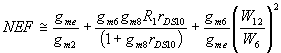 (4.7)
(4.7)
In fig.4.7, NEF has been represented as a function of aspect ratios of transistors MN12 and MN6 at different coarse tuning conditions.
|
|
|
Fig.4.7: The noise excess factor of the transconductor |
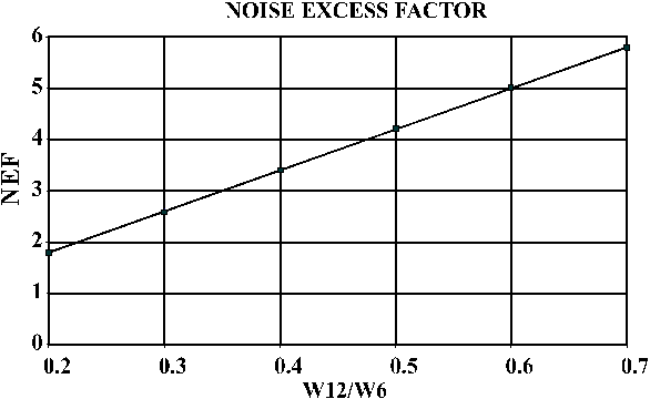
At maximum transconductance, the noise excess factor is closed to 6. The noise of the transconductor has been optimized by using W scaling. After scaling, simulations show a total in-band noise of 158m Vrms.
4.2.7. Dynamic range and power
Consider the unity feedback configuration and the procedure from section 3.4.5 for G=1. Denote h the power efficiency of the transconductor related to the transconductance of the input stage and NEF its noise excess factor. The minimal power consumption for a unity feedback configuration when, the power supply is larger than the saturation limits of the PMOS and NMOS cascoded outputs is:
 (4.8)
(4.8)
For comparisons with other low-voltage transconductors we need a factor of merit in which dynamic range, THD power and tuning are taken into account. In [8] a factor of merit for transconductors has been defined:
![]() (4.9)
(4.9)
In the factor of merit FOM, V2in,RMSmax represents the maximum rms value of the input voltage and P the total power needed to bias the complete circuit. The figure of merit was defined under the conditions of maximum tuning and total harmonic distortion of about -50dB in worst-case condition for noise excess factor NEF. Given the dynamic range of the transconductor :
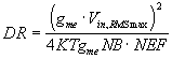 (4.10)
the factor of merit FOM equals DR/4KT× P ratio for a noise bandwidth NB of 1Hz. The figure of merit is determined under the following conditions:
- The transconductance is 30m A/V;
- NEF=6;
- The rms input voltage for THD=-50dB is 1.41Vrms
- P=1.48mW at VDD=3.3V
This results in a figure of merit of about 6.7× 10⁻³. FOM is ten times better than FOM of the transconductor from references [9] and [10] which has a value of 0.7× 10⁻³ and has been implemented in the same technology. The difference comes from the larger input swing allowed in this design and its linearity. In conclusion large voltage swings at low supply voltage is proven beneficial to achieve high dynamic range and large DR/P ratios.
|
|
|
Fig.4.8: Circuit diagram of the transconductor |