Low-noise, low residual offset, chopped amplifiers for high-end applications
6.3. The gain stage
One of the requirements of the amplifier is that a low-ohmic load has to be connected to the output of the opamp. Therefore, large output transistors are needed to supply the large output currents. The output stage does not have a large gain. The amplifier is divided in two sections: a high gain section and an output section containing an output stage with a high current drive capability. In fig.6.3 the position of the output stage is after the second chopper. Therefore, the noise and the offset of the output stage can become dominant in the total noise/offset term. As long as the gain of the input stage is sufficiently high, the offset/noise contribution of the output stage can be made negligible small. Another reason to have large gain comes from the attenuation of signal in the class AB output stage which can be as high as 30dB. Fig.6.4 illustrates the input stage of the opamp. The reason to chose a PMOS input stage comes from the necessity to reduce the influence of the substrate noise.
|
|
|
Fig.6.4: The gain stage of the opamp |
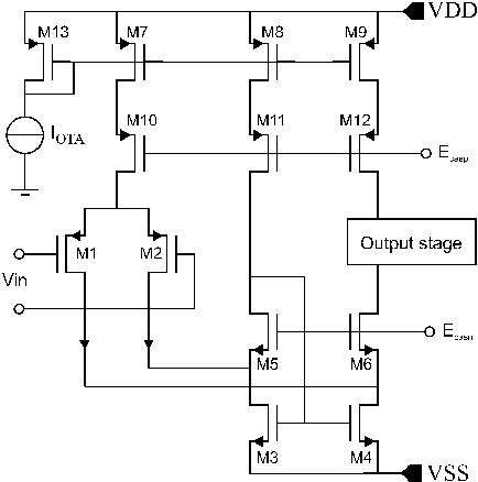
The two transistors are in a N-well and the well is connected to the supply voltage such that any substrate interference coupled via the parasitic capacitance to substrate is decoupled to VDD line. The opamp has a single-ended output. The chopper modulators need a differential signal but the required single-ended output imposes the use of a differential to single-ended conversion. This is discussed in the next paragraphs.
In fig.6.5 different possible solutions for differential to single ended conversion are depicted. The circuit from fig.6.5.a has been already presented in the previous chapter. The input differential signal current x is injected at the source of M3 and M4. The mirror in top will perform the differential to single ended conversion while M1 and M2 are in saturation and providing the necessary biasing. Chopping at low impedance nodes as shown in the case of the OTA from previous chapter means chopping three times in the signal path. Charge injection in the third modulator is a common mode interference as long as the current mirror has infinite bandwidth. However, the limited bandwidth of the mirror decreases the common mode rejection properties of the circuit.
The circuit from fig.6.5.b performs the conversion without the need of a PMOS mirror. M1 and M2 are working in the linear region and the signal conversion is performed at the drain of M2. The cross-quad M3…M6 keeps the drains of the transistors M1 and M2 in steady state at the same voltage, minimizing the systematic offset of the opamp. Besides, it provides a high output impedance needed for large gains. The disadvantage is the large voltage needed at the output node to keep M3…M6 in saturation. In order to drive the output transistors from the class AB stage close to cutoff, we need large swings at the output node of the gain stage. The two current sources I0 from the top are dynamically matched.
|
|
|
Fig.6.5: Differential to single ended converters |
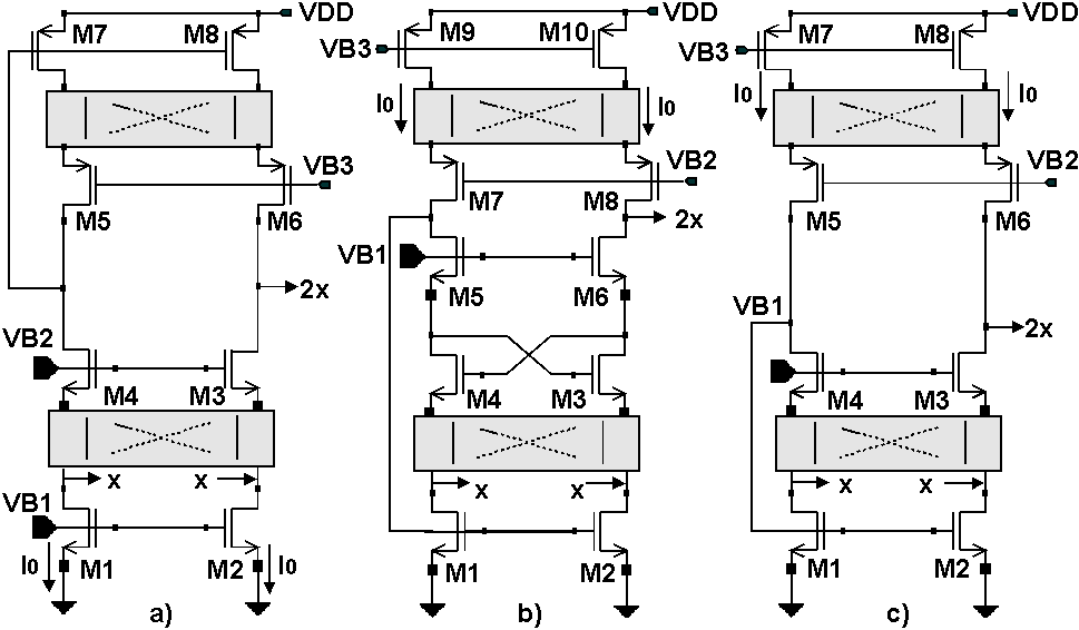
Fig.6.6.c shows the differential to single ended converter employed in the design of the gain stage. By using this stage, there is no need for a PMOS current mirror in the signal path. We are chopping only twice in the signal path and the accuracy of the current sources Io can be improved by using dynamic element matching. Compared to the previous solution we can have larger swings at the output 2x while chopping only twice in the signal path.
The choice of the output stage has to be made in conformity to the low voltage requirements. The source follower configuration from fig.6.6.a gives always a voltage drop of about one VT to the supply rails and therefore the maximum possible output swing could never be reached. The rail-to-rail configuration from fig.6.6.b has a close to rails swing. The disadvantage is that the gain depends strongly on the load and the transconductance of the output transistors.
|
|
|
Fig.6.6: The output stage with class AB control |
