Low-noise, low residual offset, chopped amplifiers for high-end applications
6.5. A low noise, low residual offset, chopped amplifier in 0.5
mm CMOSThis section presents a low noise, low residual offset, chopped amplifier in 0.5mm CMOS technology. It consists of a chopped transconductance stage and a new class AB stage capable of working at 1.3V supply voltage. By using gain boosting and low voltage techniques, the gain of the amplifier is boosted at 91dB for a 32W load.
6.5.1. The class AB control circuit
The chopped amplifier is divided in two parts: the gain stage and the output stage capable of driving low-ohmic loads. To be able to go to lower supply voltages, a new class AB control circuit is introduced. The output stage is shown in fig.6.21 and consists of an input common-mode current source of the pair M14 and M15, with active load, and the class AB control circuit. The output transistors M35, M36 are driven in phase from high impedance nodes. To control the output currents, a
|
|
|
Fig.6.21: Class AB output stage |
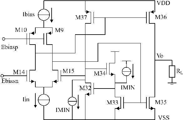
feedback control has been chosen. A scaled copy of the current in the output devices flows through M33 and M37. The two copies are forced in the transistors M34 and M32. The feedback loop around the differential amplifier M14 and M15 will enforce the condition:
![]()
The transistors M34 and M35 can work in weak inversion or strong inversion. In both situations the class AB control is effective.
a. Weak inversion behavior
If the transistors M34 and M32 are well matched and at the same temperature in weak inversion, forward saturated (VDS>>UT), then the condition (6.4) can be rewritten as:
![]()
where n is the slope factor, UT is
the thermal voltage, b represents the gain factor, m the scaling factor and KW is a dimensionless constant. This condition holds true as long as mI35,36>IMIN. The constant KW depends on technology and some physics constants. (6.6)
(6.6)
In eq. (6.6) y 0 represents the surface potential and f F the Fermi level potential. In most cases, the constant KW can be approximated with:
![]() (6.7)
(6.7)
The transistors M32 and M34 are considered matched and at the same temperature. The body effect has been neglected. One can see that for a given temperature, the product of the left hand side terms from (6.5) is constant.
The class AB behavior has been simulated and shown in fig.6.22. If only the product rule would have been implemented, the residual current is not limited. Hence, if one of the transistors would conduct a lot of current the other one works at very low currents and the gate-source voltage associated with it becomes low. The circuit that drives the gates of the output transistors should have some 500¸ 600mV voltage room to keep all of its transistors in saturation. That is why, in this approach we need a well defined residual current in the output transistors. The two extra current sources IMIN subtract a small current from the copied output currents coming from M33 and M37. This causes in all situations a shift upwards for the current flowing in the output transistors providing the required minimum current.
- Strong inversion behavior
If the transistors M34 and M32 are working in strong inversion the class AB control of the output transistors is also valid. This time the condition (6.4) can be rewritten as:
![]() (6.8)
(6.8)
This equation is valid if only mI35,36>IMIN.
|
|
|
Fig.6.22: The simulated class AB currents in the output transistors |

6.5.2. Circuit principle
The final version of the circuit is illustrated in fig.6.21. The weak inversion variant of the class AB control has been chosen for implementation. The large bandwidth mirror M7, M8, M13, M14 and M15 used for differential to single ended conversion, is being chopped at low impedance nodes.
The single ended signal current generated at the output of the mirror acts as a common-mode current of the differential pair M14 and M15 being divided afterwards in two branches. Due to the equal splitting, the output transistors M36 and M35 are driven in phase. The only sources of offset and 1/f noise remains the output stage and mismatches between the two signal branches. There are few reasons to desire a high gain for the transconductance stage. For low ohmic loads, the output stage attenuates the signal up to -12dB. Hence, the open loop gain of the amplifier drops down. If the transconductance stage has large gain, the offset and 1/f noise generated in the output stage can be neglected.
In modern processes, the output resistance of the transistors is very low. Simple cascoding does not offer a solution in this case because of the large voltage headroom needed. Besides, we want large swings at the output nodes of the transconductance stage in order to ensure that output transistors are driven out of saturation for large swings. A gain boosting circuit M16, M17, M22 and M23 has been added to the cascode transistors M18, M19, M20 and M21. Its current consumption is limited to few nanoamperes and the noise and offset of the gain boosting transistors is negligible.
At the output node, we can go as low as VGS16+VGS18-VT. Because the gain boosting transistor works at low current, in weak inversion, the gate-source voltage of M16 is close to VT and therefore we can go as low as 600mV from the ground rail. The same applies to the PMOS counterparts. The gate of the transistor M14 is connected to a constant voltage and the differential amplifier will enforce a constant voltage at the gate of M16. The gain boosting circuit limits the minimum supply voltage at about 1.4V :
![]()
|
|
|
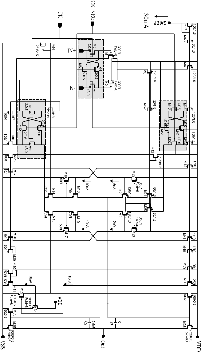
Fig.6.23: The circuit diagram |
|
|
|
Fig.6.24: The simulated frequency transfer |

6.5.3. Simulation results
The circuit has been simulated by using a 0.5mm CMOS process. A worst case situation with a low ohmic load of 32W has been considered in all cases. The opamp is compensated with two Miller capacitors of 5pF and 2.5pF, respectively, to account for the area differences of the two output transistors M35 and M36.
a. Open loop gain and stability
The open loop gain of the circuit is presented in fig.6.24 under the condition of a heavy load of 32W ç ç 5pF and 32W ç ç 300pF load capacitance, respectively. The opamp has a gain bandwidth product of 1.8MHz, 91dB low frequency gain and the phase margin is 87 degree and 83 degree respectively.
By steering the output transistors in triode region, to have a close to rail output, instability could occur. This is caused by the decrease of the gain and the shift of the second pole of the amplifier. In order to prove that the circuit is stable in all possible situations, a transient analysis has been performed for different amplitudes at the output as shown in fig.6.25 This simulation has been done with different possible amplitudes of the signal in a follower configuration and shows no ringing or overshoot at the output. For a 32W load, the maximum output voltage is close to the rails within 360 millivolts.
Fig.6.26 illustrates the spectral density of the input referred voltage noise for the two opamps. In the case of the opamp implemented in a 0.5mm CMOS process, the 1/f noise properties are worse in comparison to the opamp implemented in 0.8 mm CMOS, although the dimensions of the input transistors are the same and the input
|
|
|
Fig.6.25: Transient response |

stage is biased at the same current level. We have mentioned in Chapter 3 that in deep sub-micron technologies, the transistor effect takes place more at the surface and therefore the 1/f noise will increase. The spectral density of the white noise in both cases is 27nV/Ö Hz.
Offset simulations show a static offset of 1.67mV. Chopping at 10MHz, the simulated residual offset is 450m V but at 1KHz chopping, the simulated residual offset is about 10m V. Given the fact that 1/f noise is reduced by chopper modulators and the white noise has the same spectral density at low frequencies we can conclude that after chopping, the two designs have the same noise power in the audio band. For the same supply voltage, the signal power is higher in this case due to large voltage swings allowed at the output.
|
|
|
Fig.6.26: Spectral density of the input noise |

|
|
|
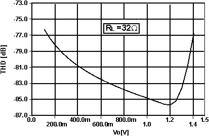
Fig.6.26: THD vs. amplitude |
c. Linearity simulations
The linearity of the opamp depends on the load and frequency. In fig.6.26 the THD as a function of the output amplitude is shown. This simulation was done at 1KHz input frequency and 32W load resistance. THD is better than -85dB for signal amplitudes close to 2.4Vpp. At low signal amplitudes the cross-over distortion takes over and the linearity gets worse. At high amplitudes clipping occurs and again the harmonic distortion increases. In fig.6.27 the THD versus frequency has been considered. The amplitude of the signal is close to 2.4Vpp and the load resistance is 32W . As expected, the harmonic distortion increases at higher frequencies due to the reduction of the loop gain. The power consumption of the opamp is 1.5mW from a 3.3V power supply voltage being dominated by the power consumption of the class AB output stage.
|
|
|
Fig.6.27: THD vs. frequency |

The opamp can work down to 1.4V with reduced swing and dynamic range. A summary of the simulated performance is shown in Table 6.2.
|
PARAMETER |
VALUE |
|
AV0 ç 32W ç ç 300pF |
91dB |
|
PM|32W ç ç 300pF |
83° |
|
GBW |
1.8MHz |
|
THDç 1kW ,1KHz |
90dB |
|
THDç 32W ,1KHz |
83dB |
|
VOS,STATIC |
<1.67mV |
|
VOSç fchop=10MHz |
<450m V |
|
VOSç fchop=1KHz |
10m V |
|
VNOISE, THERMAL |
27nV/Ö Hz |
|
SUPPLY |
3.3V± 10% |
|
VDD, MIN |
1.4V |
|
P |
1.5mW |
|
Technology |
0.5m m, 2PS,3AL, CMOS |
Table 6.2: Summary of performance