A 16-bit D/A interface with Sinc approximated semidigital reconstruction filter
7.4. Semidigital FIR filter principles
Consider fig.7.6 where the basic principle of the current driven D/A interface is shown [11]. As explained in section 6.2, it consists of a FIR semidigital filter with 1
|
|
|
Fig.7.6: Basic principles |
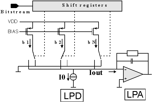
bit digital delay units and analog tap weights followed by an analog post-filter [14]. The input of the D/A interface is a bitstream signal already noise-shaped. The current source I0 needed to prescribe the common mode level at the input introduces noise. Integrating on the same chip analog and digital circuits, the substrate noise can become a problem in the single ended approach.
That is why we have introduced the differential D/A from fig.7.7. The 1-bit output of the noise-shaper with a sample frequency of 2.8MHz will pass through the 1-bit digital delay units implemented with shift-registers. The outputs of the shift registers are controlling the switches of the current taps directing the current to the negative or positive input of the opamp. The noise-shaper and the upsampling filter are not integrated on the same chip. The FIR filter has unity transfer for the baseband signal, with minimum ripple and attenuates the out-of-band quantization noise. Due to oversampling, the analog post-filter can be simply reduced to a first order filter thus simplifying the integration on-chip of the digital and analog functions.
The coefficients of the filter implemented with weighted current sources, have the property that ak=aN-k+1. The filter is symmetrical with respect to the middle coefficient. Due to the differential approach if a current DI is flowing towards the positive input of the opamp, a negative current -DI is flowing towards the negative input of the opamp. Therefore, the current is not being dumped to ground as will be in the case of single-ended solutions [see fig.7.6]. The differential approach has been used to make larger voltage swings at the output. The effect of digital crosstalk and the glitches in the output current will be minimized. Given the data x[n] at the input of the shift registers, the currents at the input of the opamp are:


|
|
|
Fig.7.7: Basic principles |
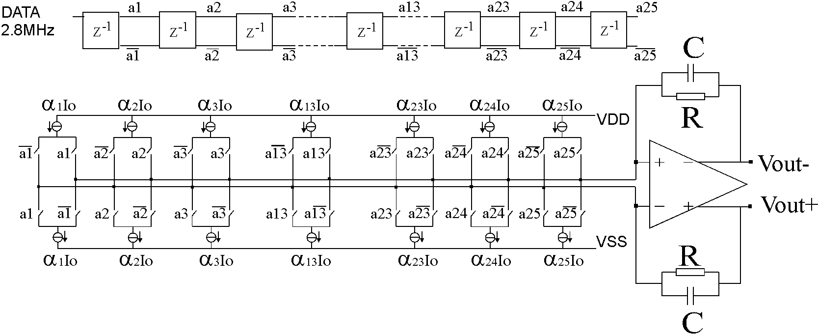
The filter coefficients are implemented by using current sources with different weights ak The output of the shift-registers is time continuous due to the holding property. During sampling interval, the current is delivered continuously to the output of the FIR and therefore zero-order hold effect is being encountered. The analog continuous-time first order RC filter attenuates further the ripple present in the output of the FIR filter. Given the pole of the low-pass filter fp and the sampling frequency fs the total transfer function of the FIR and continuous time analog filter including the zero-order hold effect will be:
 (7.11)
The total transfer is considered when the coefficients of the filter are being calculated. The cutoff frequency of the low-pass filter should be chosen such that the pass-band response is not impaired.