A 16-bit D/A interface with Sinc approximated semidigital reconstruction filter
7.8. Experimental results
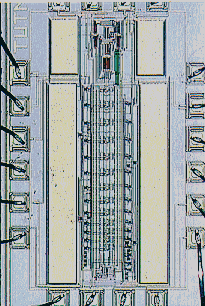
The D/A interface has been realized in a 0.8mm CMOS 5V technology with two metal layers and one polysilicon layer. Fig.7.26 illustrates the chip photomicrograph. The active area of the circuit is 1.6mm2 being dominated by capacitances needed for low-pass filtering and compensation. Extreme care has been taken for matching the current sources in the lay-out. During the measurements, the RTZ signal was set to VDD. For measurement purposes, a bitstream signal has been used as a DATA input. Fig.7.27 shows the signal to noise and distortion measurement (S/N+THD) for a sine input at 1KHz. Here, the noise floor is around -115dB…-120dB and the distortion peaks are lower than -87dB. The total harmonic distortion is -86dB at 1KHz input and the even order distortion components give the largest contribution at the output.
|
|
|
Fig.7.26: Chip photomicrograph |
|
|
|
Fig.7.27: S/N+THD measurement at 1KHz FS |

The setup for the spectrum measurements had a single ended input. This explains the unexpected increase in the even order harmonics. Table 7.2 shows the performance summary of the D/A interface.
|
PARAMETER |
VALUE |
|
Technology |
0.8m m, 1PS, 2AL, CMOS |
|
Supply voltage |
5V |
|
Area |
1.6mm2 |
|
Opamp AOL |
90dB (RL=10KW ) |
|
GBW |
40MHz |
|
Phase margin |
75° |
|
Slew rate |
5V/m s |
|
Output swing |
9.8Vpp |
|
DR opamp |
103dB |
|
THD|RL=10kW |
-86dB @ f=1KHz |
|
Power consumption |
20mW |
Table 7.2: Summary of performance