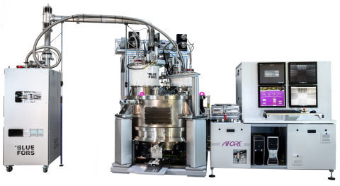
SANTA CLARA, Calif. — (BUSINESS WIRE) — February 28, 2019 — What’s New: Intel, Bluefors* and Afore* have introduced the first cryoprober, a quantum testing device named the Cryogenic Wafer Prober, developed specifically to speed the development of quantum computing solutions. Intel identified the need for a quantum testing tool to collect more data about quantum chips called “qubits.”
This press release features multimedia. View the full release here: https://www.businesswire.com/news/home/20190228005173/en/

Built by Intel, Bluefors and Afore, the first Cryogenic Wafer Prober is a cryoprober tool designed to test and validate qubits needed for quantum computing. The Cryogenic Wafer Prober allows researchers to test qubits on 300mm wafers down to temperatures of a few kelvins, making it a first-of-its-kind testing tool for quantum computing. The first Cryogenic Wafer Prober will be located at Intel’s Oregon campus. (Credit: Intel Corporation)
“Building on our expertise in transistor process technology, we saw
the need to create a 300mm high-volume fabrication and test line for
semiconductor spin qubits. We are focused on the manufacturability and
scaling issues for quantum, and a fast feedback through the cryoprober
allows Intel to accelerate our scientific learning.”
–Dr. Jim
Clarke, director of Quantum Hardware, Intel
Why It Matters: One of the biggest challenges with quantum computing is data collection and access to data. Today, each quantum processor is tested for months in a low-temperature dilution refrigerator to determine what works and what doesn’t work.
Conventional transistors are very different, and with the right tools, Intel can characterize a large subset of these transistors on a 300mm wafer in about an hour and rapidly inform the feedback loop back to the fabrication line. For quantum computing, however, the turn-on characteristics of qubits must be measured at low temperatures of less than a few kelvins above absolute zero. Until now, the electrical characterization of qubits was very slow compared with traditional transistors, often taking days to collect even small subsets of data.
How It Works: Intel approached Bluefors, a leader in building cryogen-free dilution refrigerator systems with a strong focus on quantum computing, who partnered with Afore, a leading micro-electro-mechanical systems (MEMS) test solutions provider based in Finland, to design and manufacture the device. The Cryogenic Wafer Prober allows researchers to test qubits on 300mm wafers down to temperatures of a few kelvins, making it a first-of-its-kind testing tool for quantum computing. The first Cryogenic Wafer Prober will be located at Intel’s Oregon campus next to several quantum computing dilution refrigerators.
“So far the past year, Intel has worked with Bluefors and Afore to combine our expertise and build a fast, electrical characterization tool that can operate in the quantum regime. We hope that by designing this tool, the industry can use it to accelerate the progress of quantum computing,” Clarke said of the project.
“Intel approached us more than a year ago, looking for a tool with the possibility to probe 300mm wafers at temperatures of only a few kelvins,” said Dr. David Gunnarsson, Bluefors chief sales officer and principal scientist. “This was indeed a challenge, and to be able to take on a tool like this, we reached out to another Finnish company, Afore, which has long experience in specialized wafer probe systems. Together we came up with a design for a tool, the cryogenic wafer prober, which we now have constructed and assembled. We are looking forward in excitement to see the advances this tool will bring to the future of quantum computing.”
This tool allows Intel to automate and collect information on spin qubits, including sources of quantum noise, the quality of quantum dots and the materials that matter in building spin qubits in a matter of minutes versus weeks.
What Early Testing Data Show: In a first demonstration of the utility of the Cryogenic Wafer Prober, Intel measured the electrical turn-on characteristic for more than 100 qubit structures across a wafer fabricated at Intel’s silicon qubit fabrication flow on its 300mm processing line in Oregon. The attached graphic illustrates the tool’s novel ability to collect high-volume cryogenic data and create a statistical correlation of the increase in turn-on voltage between room temperature and cryogenic temperature. With this tool, Intel will be able to speed feedback into the silicon spin qubit fabrication line and accelerate quantum computing research and development.
More Context: The Cryogenic Wafer Prober | Quantum Computing at Intel | Intel Labs
About Intel
Intel (NASDAQ: INTC), a leader in the semiconductor industry, is shaping the data-centric future with computing and communications technology that is the foundation of the world’s innovations. The company’s engineering expertise is helping address the world’s greatest challenges as well as helping secure, power and connect billions of devices and the infrastructure of the smart, connected world – from the cloud to the network to the edge and everything in between. Find more information about Intel at newsroom.intel.com and intel.com.

