New V-NAND breaks through current cell stacking limitation in 3D NAND with the industry's first 100+ layer single-tier design for superior speed and power efficiency
Starting with a 250GB SATA SSD now in production, Samsung plans to offer high-speed, high-capacity SSDs and eUFS solutions based on its sixth-generation V-NAND
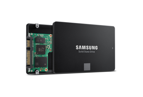
SEOUL, Korea — (BUSINESS WIRE) — August 6, 2019 — Samsung Electronics Co., Ltd., the world leader in advanced memory technology, today announced that it has begun mass producing 250-gigabyte (GB) SATA solid state drive (SSD) that integrates the company’s sixth-generation (1xx-layer) 256-gigabit (Gb) three-bit V-NAND for global PC OEMs. By launching a new generation of V-NAND in just 13 months, Samsung has reduced the mass production cycle by four months while securing the industry’s highest performance, power efficiency and manufacturing productivity.
This press release features multimedia. View the full release here: https://www.businesswire.com/news/home/20190806005360/en/

Samsung Electronics Takes 3D Memory to New Heights with Sixth-generation V-NAND SSDs for Client Computing (Photo: Business Wire)
“By bringing cutting-edge 3D memory technology to volume production, we are able to introduce timely memory lineups that significantly raise the bar for speed and power efficiency,” said Kye Hyun Kyung, executive vice president of Solution Product & Development at Samsung Electronics. “With faster development cycles for next-generation V-NAND products, we plan to rapidly expand the markets for our high-speed, high-capacity 512Gb V-NAND-based solutions.”
The only single-stack 3D memory die with a 100+ layer design
Samsung’s sixth-generation V-NAND features the industry’s fastest data transfer rate, capitalizing on the company’s distinct manufacturing edge that is taking 3D memory to new heights.
Utilizing Samsung’s unique ‘channel hole etching’ technology, the new V-NAND adds around 40-percent more cells to the previous 9x-layer single-stack structure. This is achieved by building an electrically conductive mold stack comprised of 136 layers, then vertically piercing cylindrical holes from top to bottom, creating uniform 3D charge trap flash (CTF) cells.
As the mold stack in each cell area increases in height, NAND flash chips tend to become more vulnerable to errors and read latencies. To overcome such limitations, Samsung has incorporated a speed-optimized circuit design that allows it to achieve the fastest data transfer speed, at below 450 microseconds (μs) for write operations and below 45μs for reads. Compared to the previous generation, this represents a more than 10-percent improvement in performance, while power consumption is reduced by more than 15 percent.
Thanks to this speed-optimized design, Samsung will be able to offer next-generation V-NAND solutions with over 300 layers simply by mounting three of the current stacks, without compromising chip performance or reliability.
In addition, the number of channel holes required to create a 256Gb chip density has decreased to 670 million holes from over 930 million with the previous generation, enabling reduced chip sizes and less process steps. This brings a more than 20-percent improvement in manufacturing productivity.
Leveraging the high-speed and low-power features, Samsung plans to not only broaden the reach of its 3D V-NAND into areas like next-generation mobile devices and enterprise servers, but also into the automotive market where high reliability is extremely critical.
Following today’s introduction of the 250GB SSD, Samsung plans to offer 512Gb three-bit V-NAND SSD and eUFS in the second half of this year. The company also expects to expand production of higher-speed and greater-capacity sixth-generation V-NAND solutions at its Pyeongtaek (Korea) campus starting next year to better meet demand from global customers.
Reference: Samsung V-NAND mass production timeline
Date |
V-NAND |
July 2013 |
1st-generation (24-layer) 128Gb MLC V-NAND |
Aug. 2013 |
1st-generation 128Gb MLC V-NAND 960GB SSD |
Aug. 2014 |
2nd-generation (32-layer) 128Gb 3-bit V-NAND |
Sept. 2014 |
2nd-generation V-NAND SSD |
Aug. 2015 |
3rd-generation (48-layer) 256Gb 3-bit V-NAND |
Sept. 2015 |
3rd-generation V-NAND SSD '850 EVO', '950 PRO' |
Dec. 2016 |
4th-generation (64-layer) 256Gb 3-bit V-NAND |
Jan. 2017 |
4th-generation V-NAND SSD |
Jan. 2018 |
4th-generation 512Gb V-NAND 30.72TB SAS SSD |
May 2018 |
5th-generation (9x-layer) 256Gb 3-bit V-NAND |
June 2018 |
5th-generation V-NAND SSD |
June 2019 |
6th-generation (1xx-layer) 256Gb 3-bit V-NAND |
July 2019 |
6th-generation V-NAND SSD |
###
About Samsung Electronics Co., Ltd.
Samsung inspires the world and shapes the future with transformative ideas and technologies. The company is redefining the worlds of TVs, smartphones, wearable devices, tablets, digital appliances, network systems, and memory, system LSI, foundry and LED solutions. For the latest news, please visit the Samsung Newsroom at http://news.samsung.com.
View source version on businesswire.com: https://www.businesswire.com/news/home/20190806005360/en/
Contact:
Ujeong Jahnke
Samsung Semiconductor Europe GmbH
Tel. +49(0)6196-66-3300
Email:
Email Contact

