The new technology allows for the stacking of 12 DRAM chips using more than 60,000 TSV holes, while maintaining the same thickness as current 8-layer chips
SEOUL, South Korea — (BUSINESS WIRE) — October 7, 2019 — Samsung Electronics Co., Ltd., a world leader in advanced semiconductor technology, today announced that it has developed the industry's first 12-layer 3D-TSV (Through Silicon Via) technology.
This press release features multimedia. View the full release here: https://www.businesswire.com/news/home/20191007005298/en/

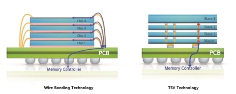
Wire bonding vs TSV technology (Graphic: Business Wire)
Samsung's new innovation is considered one of the most challenging packaging technologies for mass production of high-performance chips, as it requires pinpoint accuracy to vertically interconnect 12 DRAM chips through a three-dimensional configuration of more than 60,000 TSV holes, each of which is one-twentieth the thickness of a single strand of human hair.
The thickness of the package (720㎛) remains the same as current 8-layer High Bandwidth Memory-2 (HBM2) products, which is a substantial advancement in component design. This will help customers release next-generation, high-capacity products with higher performance capacity without having to change their system configuration designs.
In addition, the 3D packaging technology also features a shorter data transmission time between chips than the currently existing wire bonding technology, resulting in significantly faster speed and lower power consumption.
“Packaging technology that secures all of the intricacies of ultra-performance memory is becoming tremendously important, with the wide variety of new-age applications, such as artificial intelligence (AI) and High Power Computing (HPC)," said Hong-Joo Baek, executive vice president of TSP (Test & System Package) at Samsung Electronics.
"As Moore's law scaling reaches its limit, the role of 3D-TSV technology is expected to become even more critical. We want to be at the forefront of this state-of-the-art chip packaging technology."
Relying on its 12-layer 3D-TSV technology, Samsung will offer the highest DRAM performance for applications that are data-intensive and extremely high-speed.
Also, by increasing the number of stacked layers from eight to 12, Samsung will soon be able to mass produce 24-gigabyte (GB)* High Bandwidth Memory, which provides three times the capacity of 8GB high bandwidth memory on the market today.
Samsung will be able to meet the rapidly growing market demand for high-capacity HBM solutions with its cutting-edge 12-layer 3D TSV technology and it hopes to solidify its leadership in the premium semiconductor market.
###
*8GB mass-production product= 8Gb x 8 layers, 24GB developed product= 16Gb x 12 layers
About Samsung Electronics Co., Ltd.
Samsung inspires the world and shapes the future with transformative ideas and technologies. The company is redefining the worlds of TVs, smartphones, wearable devices, tablets, digital appliances, network systems, and memory, system LSI, foundry and LED solutions. For the latest news, please visit the Samsung Newsroom at http://news.samsung.com.
View source version on businesswire.com: https://www.businesswire.com/news/home/20191007005298/en/
Contact:
Ujeong Jahnke
Samsung Semiconductor Europe GmbH
Tel. +49(0)6196-66-3300
Email:
Email Contact

