TORRANCE, Calif., Nov. 01, 2022 (GLOBE NEWSWIRE) --
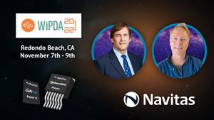
Navitas Semiconductor (Nasdaq: NVTS), the industry leader in gallium nitride (GaN) power ICs and silicon carbide (SiC) technologies, has announced that Dan Kinzer, the company’s co-founder and COO/CTO, will present a keynote speech on next-generation semiconductor technology at the forthcoming IEEE WiPDA (Wide Bandgap Power Devices & Applications) workshop.
Taking place from November 7th-9th 2022, the ninth WiPDA Workshop provides a forum for device scientists, circuit designers and application engineers from the Power Electronics & Electron Devices Societies to share wide bandgap (WBG) technology updates, research findings, experience and potential applications.
Mr. Kinzer’s keynote “High-speed GaN and SiC: $22B of pure-play power semiconductors” spotlights key market drivers and technology developments in GaN and SiC as they continue to displace legacy silicon in a growing range of applications including mobile ultra-fast chargers, data centers, renewables and EVs.
An additional technical paper, “Advancement in Integration for GaN Power ICs: Autonomous Protection and Loss-Less Sensing”, will be presented by Tom Ribarich, Navitas’ Sr. Director Strategic Marketing.
Navitas’ latest family of 650 V GaNSense half-bridge ICs offer a revolutionary step forward in integration, integrating two GaN FETs with drive, control, sensing, autonomous protection, and level-shift isolation. This single-package solution reduces component count and footprint by over 60% compared to existing discretes, which cuts system cost, size, weight, and complexity.
Additionally, new GeneSiC MOSFETs range from 750 V to 6.5 kW, and deliver the industry’s highest figures-of-merit for high temperature, high-speed switching. Trench-assisted planar-gate MOSFETs, enabling 30% energy savings, 25°C cooler operation and 3x longer life. The SiC portfolio is completed with a broad range of high-performance Schottky MPS™ diodes, from 650 V to 3.3 kV.
“The IEEE WiPDA Workshop is a prestigious event, and it is a great honor to be asked to share key insights with leading experts in the field of WBG technologies,” said Mr. Kinzer. “Navitas delivers critical technological advantages in a $22 billion market opportunity.” For 30 years, Mr. Kinzer has led R&D at semiconductor and power electronics companies at the VP level or higher. His experience includes developing advanced power device and IC platforms, wide bandgap GaN and SiC device design, IC and power device fabrication processes, advanced IC design, semiconductor package development and assembly processes, and design of electronic systems. Before co-founding Navitas, Mr. Kinzer served as VP R&D, VP Advanced Product Development, and Chief Technologist at International Rectifier (IR sold to Infineon for $3B), and SVP Product & Technology Development & CTO at Fairchild Semiconductor (Fairchild sold to onsemi for $2.4B). He holds over 180 US patents, and a BSE degree in Engineering Physics from Princeton University.
IEEE WiPDA 2022 takes place at the Sonesta Redondo Beach and Marina, from November 7th-9th. To register, please visit https://wipda.org/registration/ . To meet with the Navitas team, please email info@navitasemi.com .
About IEEE WiPDA
Sponsored by the IEEE Power Electronic Society (PELS), the IEEE Electron Devices Society, and the Power Sources Manufacturers Association (PSMA), the annual IEEE Workshop on Wide Bandgap Power Devices and Applications (WiPDA) is one of the key gatherings for the WBG technical community. The ninth workshop allows device scientists, application and system engineers, university professors and students to share and exchange information on their recent research findings, report on key results and discuss the main challenges for both gallium nitride (GaN) and silicon carbide (SiC) based technologies, devices, applications and systems.
About Navitas
Navitas Semiconductor (Nasdaq: NVTS) is the only pure-play, next-generation power-semiconductor company, founded in 2014.
GaNFast™ power ICs integrate gallium nitride (GaN) power and drive, with control, sensing, and protection to enable faster charging, higher power density, and greater energy savings. Complementary
GeneSiC™ power devices are optimized high-power, high-voltage, and high-reliability silicon carbide (SiC) solutions. Focus markets include mobile, consumer, data center, EV, solar, wind, smart grid, and industrial. Over 185 Navitas patents are issued or pending. Over
50 million GaN units have been shipped with zero reported GaN field failures, and Navitas introduced the industry’s first and only 20-year warranty. Navitas is the world’s first semiconductor company to be
CarbonNeutral®-certified.
Navitas, GaNFast, GaNSense, GeneSiC, and the Navitas logo are trademarks or registered trademarks of Navitas Semiconductor and subsidiaries. All other brands, product names, and marks are or may be trademarks or registered trademarks used to identify products or services of their respective owners.
Contact Information:
Stephen Oliver, VP Corporate Marketing & Investor Relations,
ir@navitassemi.com
A photo accompanying this announcement is available at https://www.globenewswire.com/NewsRoom/AttachmentNg/c615054c-a3ee-495b-9b11-5ae264075576


