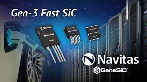
TORRANCE, Calif., June 06, 2024 (GLOBE NEWSWIRE) -- Navitas Semiconductor (Nasdaq: NVTS), the industry leader in next-generation GaNFast™ gallium nitride (GaN) and GeneSiC™ silicon carbide (SiC) power semiconductors, announces their new portfolio of Gen-3 ‘Fast’ (G3F) 650 V and 1,200 V SiC MOSFETs optimized for fastest switching speed, highest efficiency, and increased power density for applications such as AI data center power supplies, on-board chargers (OBCs), fast EV roadside super-chargers, and solar / energy-storage systems (ESS). The broad portfolio range covers industry-standard packages from D2PAK-7 to TO-247-4, designed for demanding, high-power, high-reliability applications.
The G3F family is optimized for high-speed switching performance, resulting in 40% improvement to hard-switching figures-of-merits (FOMs) compared to competition in CCM TPPFC systems. This will enable increasing the wattage of next-generation AI power supply units (PSUs) up to 10 kW, and power per rack increase from 30 kW to 100-120 kW.
The G3F GeneSiC MOSFETs are developed using a proprietary ‘trench-assisted planar’ technology and offer better-than-trench MOSFET performance, while also providing superior robustness, manufacturability and cost than competition. G3F MOSFETs deliver high-efficiency with high-speed performance, enabling up to 25°C lower case temperature, and up to 3x longer life than SiC products from other vendors.
The ‘trench-assisted planar’ technology enables an extremely low RDS(ON) increase versus temperature, which results in the lowest power losses across the complete operating range and offers up to 20% lower RDS(ON) under real-life operation at high temperatures compared to competition.
Additionally, all GeneSiC MOSFETs have the highest-published 100%-tested avalanche capability, 30% longer short-circuit withstand time, and tight threshold voltage distributions for easy paralleling, GeneSiC MOSFETs are ideal for high-power, fast-time-to-market applications.
Navitas’ latest 4.5 kW high-power density AI Server PSU reference design in CRPS185 form-factor, showcases the 650 V-rated, 40mOhms G3F FETs for an Interleaved CCM TP PFC topology. Alongside the GaNSafe™ Power ICs in the LLC stage, a power density of 138 W/inch3 and peak efficiency above 97% is realized, which comfortably achieves ‘Titanium Plus’ efficiency standards, now mandatory in Europe.
For the EV market, 1,200 V/34 mOhm (G3F34MT12K) G3F FETs enable Navitas’ new 22 kW, 800V Bi-Directional OBC and 3KW DC-DC converter to achieve a superior power density of 3,5 kW/L and a peak efficiency of 95.5%.
“G3F sets a new standard for efficient, cool-running SiC performance, coupled with high-reliability and robustness for high-power, high-stress systems,” noted Dr. Sid Sundaresan, Senior Vice President of SiC Technology and Operations. “We’re pushing the boundaries of SiC, with up to 600 kHz switching speeds, and hard-switching figures-of-merit up to 40% better than competition.”
Parts are available now to qualified customers. Please contact sicsales@navitassemi.com for more information.
About Navitas
Navitas Semiconductor (Nasdaq: NVTS) is the only pure-play, next-generation power-semiconductor company, celebrating 10 years of power innovation founded in 2014. GaNFast™ power ICs integrate gallium nitride (GaN) power and drive, with control, sensing, and protection to enable faster charging, higher power density, and greater energy savings. Complementary GeneSiC™ power devices are optimized high-power, high-voltage, and high-reliability silicon carbide (SiC) solutions. Focus markets include EV, solar, energy storage, home appliance / industrial, data center, mobile, and consumer. Over 250 Navitas patents are issued or pending. Navitas was the world’s first semiconductor company to be CarbonNeutral®-certified.
Navitas Semiconductor, GaNFast, GaNSense, GeneSiC, and the Navitas logo are trademarks or registered trademarks of Navitas Semiconductor Limited and affiliates. All other brands, product names, and marks are or may be trademarks or registered trademarks used to identify products or services of their respective owners.
Contact:
Llew Vaughan-Edmunds, Senior Director of Corporate Marketing & Product Management
info@navitassemi.com
Stephen Oliver, VP of Corporate Marketing
ir@navitassemi.com
A photo accompanying this announcement is available at https://www.globenewswire.com/NewsRoom/AttachmentNg/a5982a79-e6fe-4dc3-b65c-21387cb7a9f9


