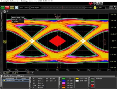
Solution reduces dynamic power consumption by up to 40 percent compared to previous generation
SAN JOSE, Calif., May 12, 2015 — (PRNewswire) — Cadence Design Systems, Inc. (NASDAQ: CDNS) today announced that its USB 3.0 host IP solution for TSMC's 16nm FinFET Plus (16FF+) process is one of the first to pass USB-IF compliance testing and receive USB-IF certification. The complete controller and PHY integrated solution is pre-verified, which enables designers to mitigate project risk and reduce system-on-chip (SoC) integration and verification time.
For more information on Cadence® IP for USB offerings, please visit: http://www.cadence.com/news/USBIP.
Cadence offers a complete USB 3.0 solution including the controller, PHY and verification IP. The certified USB 3.0 host solution for 16FF+ features an innovative architecture developed by FinFET design experts within Cadence and offers a 40 percent reduction in dynamic power consumption versus previous generations of the IP on other process nodes. To achieve this power reduction, the integrated USB host xHCI controller and PHY IP utilize power and clock gating in order to conserve energy as the USB protocol goes into a low-power sub-state. Additionally, the PHY is optimized to ease integration. With a reduced pinout, there are fewer combinations to verify and less complexity with fewer complex software interactions that need to be tested and debugged.
"For our mobile and consumer customers, achieving USB 3.0 host certification on 16FF+ is critical because it signifies a reliable and low-risk path toward successful, advanced-node SoC design," said Osman Javed, product marketing director at Cadence. "The complete solution of controller, PHY and verification IP enables customers to significantly reduce integration time and get their products to market faster. Our IP solution is available in a wide range of configurations that meets the needs of our customers looking to design for both high-performance and embedded, low-power applications."
"As a long-term member of USB Implementers Forum, Cadence delivers USB design and verification IP that reduces the integration and verification effort for today's complex SoCs," said Jeff Ravencraft, USB-IF President and COO. "USB-IF certification of IP on TSMC 16FF+ is a critical step to provide the industry with proven solutions to build interoperable, reliable USB products for consumers."
About Cadence
Cadence enables global electronic design innovation and plays an essential role in the creation of today's integrated circuits and electronics. Customers use Cadence software, hardware, IP, and services to design and verify advanced semiconductors, consumer electronics, networking and telecommunications equipment, and computer systems. The company is headquartered in San Jose, Calif., with sales offices, design centers, and research facilities around the world to serve the global electronics industry. More information about the company, its products, and services is available at http://www.cadence.com.
© 2015 Cadence Design Systems, Inc. All rights reserved worldwide. Cadence and the Cadence logo are registered trademarks of Cadence Design Systems, Inc. in the United States and other countries. All other trademarks are the property of their respective owners.
For more information, please contact:
Cadence Newsroom
408-944-7039
Email Contact

Photo - http://photos.prnewswire.com/prnh/20150511/215265
Logo - http://photos.prnewswire.com/prnh/20140102/SF39436LOGO
To view the original version on PR Newswire, visit: http://www.prnewswire.com/news-releases/cadence-usb-30-host-solution-on-tsmc-16nm-finfet-plus-process-achieves-industry-certification-300081668.html
SOURCE Cadence Design Systems, Inc.
| Contact: |
| Cadence Design Systems, Inc.
Web: http://www.cadence.com |