TOKYO — (BUSINESS WIRE) — January 25, 2018 — Toshiba Electronic Devices & Storage Corporation today announced the development of “TaRF10,” a next generation TarfSOITM (Toshiba advanced RF SOI[1]) process optimized for low-noise amplifiers (LNAs) in smartphone applications.
This press release features multimedia. View the full release here: http://www.businesswire.com/news/home/20180125006449/en/

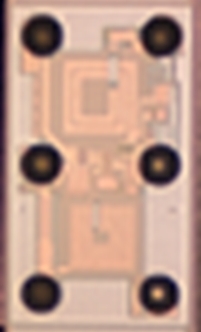
Toshiba Electronic Devices & Storage Corp.: Appearance of LNA fabricated with TaRF10 (Photo: Business Wire)
In recent years, the increasing speed of mobile data communication has expanded use of RF switches and filters in the analog front end of mobile devices. The resulting increase in signal loss between antenna and receiver circuit has degraded receiver sensitivity, and focused attention on LNAs with a low noise figure[2] (NF) as a means to compensate for signal loss and improve the integrity of the received signal.
Toshiba Electronic Devices & Storage has used its new TaRF10 process to develop a prototype LNA with an outstanding noise figure of 0.72dB and a gain[3] of 16.9dB at a frequency of 1.8GHz.
Mobile devices use many RF switches and LNAs in the receiver circuit, generating a need to reduce circuit size in order to reduce board area utilization. Current LNAs typically use silicon-germanium-carbon (SiGe: C) bipolar transistors, and it has been difficult to integrate LNAs and RF switches fabricated with different processes on the same chip.
The new TaRF10 process can integrate LNAs, control circuits and RF switches on a single chip, as it is highly compatible with the TaRF8 and TaRF9 processes for RF switches, which secure outstanding RF characteristics. TaRF9 realizes lower insertion loss and signal distortion than TaRF8. Toshiba Electronic Devices & Storage now plans to bring to market LNAs with integrated RF switches.
Toshiba Electronic Devices & Storage has developed RF ICs utilizing its
subsidiary, Japan Semiconductor Corporation to apply the latest SOI-CMOS
technology, and by handling all aspects of the production flow, from RF
process technology development to the design and manufacturing, secured
a rapid products launch.
To meet next-generation market
requirements for 5G smartphones, the company will continue to further
improve the characteristics of the TarfSOITM process and
develop RF ICs with cutting-edge technology.
|
Table 1. Main Specifications of LNA |
||||||
| Mode |
LNA applying TaRF 10
|
Unit | ||||
| Chip Size | - | 0.70×0.43 | Mm | |||
| Frequency | - | 1.8 | GHz | |||
| Supply Voltage | - | 1.8 | V | |||
| Supply Current | Gain mode | 7.4 | mA | |||
| Bypass mode | 50 | μA | ||||
| Control Voltage | Gain mode | 1.8 | V | |||
| Bypass mode | 0 | V | ||||
| Gain | Gain mode | 16.9 | dB | |||
| Bypass mode | -1.6 | dB | ||||
| NF | Gain mode | 0.72 | dB | |||
| Return Loss (In) | Gain mode | 8.4 | dB | |||
| Return Loss (Out) | Gain mode | 12.1 | dB | |||
| Reverse Isolation | Gain mode | 26.5 | dB | |||
| IP1dB | Gain mode | -8.9 | dBm | |||
| IIP3 | Gain mode | 4.3 | dBm | |||
Notes:
[1] TarfSOITM (Toshiba advanced RF SOI):
Toshiba’s unique SOI-CMOS (silicon-on-insulator-complementary metal
oxide semiconductor) front-end process
[2] Noise figure: the ratio
of signal-to-noise ratio at the output to that at the input. The lower
the noise figure, the lower the amplifier self-noise is and therefore
the better.
[3] Gain: the ratio of the output power of an amplifier
to its input power in dB
* Company names, product names, and service names mentioned herein may be trademarks of their respective companies.
Customer Inquiries:
Small Signal Device Sales & Marketing
Department
Tel: +81-3-3457-3411
https://toshiba.semicon-storage.com/ap-en/contact.html
*Information in this document, including product prices and specifications, content of services and contact information, is current on the date of the announcement but is subject to change without prior notice.
About Toshiba Electronic Devices & Storage
Corporation
Toshiba Electronic Devices & Storage
Corporation combines the vigor of a new company with the wisdom of
experience. Since being spun off from Toshiba Corporation in July 2017,
we have taken our place among the leading general devices companies, and
offer our customers and business partners outstanding solutions in
discrete semiconductors, system LSIs and HDD.
Our 19,000 employees around the world share a determination to maximize
the value of our products, and emphasize close collaboration with
customers to promote co-creation of value and new markets. We look
forward to building on annual sales now surpassing 700-billion yen (US$6
billion) and to contributing to a better future for people everywhere.
Find
out more about us at
https://toshiba.semicon-storage.com/ap-en/company.html
View source version on businesswire.com: http://www.businesswire.com/news/home/20180125006449/en/
Contact:
Media Inquiries:
Toshiba Electronic Devices & Storage
Corporation
Chiaki Nagasawa, +81-3-3457-4963
Digital Marketing
Department
Email Contact