New B6700L Tester Expands the Platform’s Temperature Range While B6700S System Offers Zero-Footprint Configuration
TOKYO, Oct. 24, 2018 (GLOBE NEWSWIRE) -- Leading semiconductor test equipment supplier Advantest Corporation (TSE: 6857) has launched two additional members of its next-generation B6700 family of burn-in memory testers. The new B6700L and B6700S models are designed to lower the cost of test while boosting the parallel testing capacity for NAND flash memories now in high demand for server and mobile data-storage applications.
“By expanding the breadth of products in our B6700 series, we are offering the global market greater flexibility to address the expected tripling of NAND storage capacity over the next few years,” said Takeo Miura, vice president of Memory ATE Business Group at Advantest. “Our two new high-volume test solutions will help customers get more return from their capital investments while retaining the ease of connecting to their existing production networks.”
The initial system in the series – the recently announced B6700D – is designed for highly parallel, low-cost testing of next-generation memories by evaluating the functionality of NAND flash devices during burn-in. Many of the system’s key features are doubled compared to its predecessor, including twice the driver-pin resources and power-supply capacity as well as a two-chamber design.
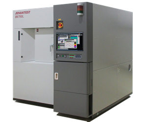
The new B6700L tester has the same resources as the B6700D while accommodating a wider temperature range. The ability to perform temperature-controlled testing from -40° C to 150° C in one-tenth of a degree increments makes this system well suited for reliability and automotive-device testing. The B6700L also can simultaneously test up to 12 B6700D-compatible burn-in boards (BIB) and test programs.
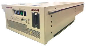
The new zero-footprint B6700S system offers a dramatically lower-cost test solution for NAND flash memories while offering the same capabilities as its sister systems. The B6700S offers a unitized function of the B6700D and can be embedded within a multi-wafer probing system used in individual wafer-level testing, avoiding any costs associated with occupying floor space in lab or production environments.
All members of the B6700 product family use the same tester boards and operating system, giving them universal compatibility. Bad block memory (BBM), universal buffer memory (UBM) and data pattern memory (DPM) functions are supported to enable NAND device testing.
The new B6700L and B6700S testers are scheduled to begin shipping to customers in the first quarter of calendar 2019.
About Advantest Corporation
A world-class technology company, Advantest is the leading producer of automatic test equipment (ATE) for the semiconductor industry and a premier manufacturer of measuring instruments used in the design and production of electronic instruments and systems. Its leading-edge systems and products are integrated into the most advanced semiconductor production lines in the world. The company also focuses on R&D for emerging markets that benefit from advancements in nanotech and terahertz technologies, and has introduced multi-vision metrology scanning electron microscopes essential to photomask manufacturing, as well as a groundbreaking 3D imaging and analysis tools. Founded in Tokyo in 1954, Advantest established its first subsidiary in 1982, in the USA, and now has subsidiaries worldwide. More information is available at
www.advantest.com.
ADVANTEST CORPORATION
3061 Zanker Road
San Jose, CA 95134, USA
Judy Davies
Email Contact
Photos accompanying this announcement are available at
http://www.globenewswire.com/NewsRoom/AttachmentNg/d14162bb-6b13-496f-b19b-24d31d83bb04
http://www.globenewswire.com/NewsRoom/AttachmentNg/ae7d4bcf-32b9-46d3-ae5e-e3c01c498581

