Cadence provides first-to-market memory model for JEDEC xSPI standard with support for Adesto EcoXiP NOR flash memory
SANTA CLARA, Calif. & SAN JOSE, Calif. — (BUSINESS WIRE) — October 1, 2019 — Adesto Technologies Corporation (NASDAQ: IOTS) and Cadence Design Systems, Inc. (NASDAQ: CDNS) today announced they have collaborated to expand the ecosystem around the Expanded Serial Peripheral Interface (xSPI) communication protocol to enable higher transfer rates and lower latency for flash memory in internet of things (IoT) devices. The Cadence® Memory Model for xSPI is the first commercially available model that allows customers to ensure optimal use of the octal NOR flash with the host processor in an xSPI system, including support for Adesto®’s EcoXiP™ octal xSPI non-volatile memory (NVM).
This press release features multimedia. View the full release here: https://www.businesswire.com/news/home/20191001005293/en/

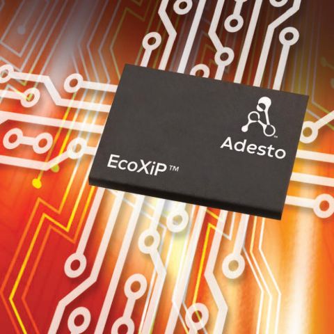
Adesto’s EcoXiP™ octal NOR flash supports xSPI to enable higher transfer rates and lower latency for IoT applications (Graphic: Business Wire)
Flash memory devices in IoT systems require increasingly higher transfer rates and lower latency, especially as these products now frequently run code-intensive wireless stacks and support local artificial intelligence (AI) processing. Expanding the flash SPI accesses from the traditional four I/Os (quad SPI) to eight I/Os (octal SPI) with the xSPI serial synchronous protocol increases the serial NOR flash throughput and provides a more efficient solution for emerging applications.
“Support for new protocols, such as xSPI, is critical for standard adoption and will help enable a new class of IoT devices,” said David Peña, verification IP product management director, System & Verification Group at Cadence. “Cadence worked closely with Adesto and other JEDEC members to drive development of the xSPI standard, and we’ve broadened our collaboration to facilitate ecosystem development. The availability of the memory model for Adesto’s EcoXiP and host controller design IP for xSPI devices enables joint customers to quickly and easily adopt xSPI while developing their products.”
One of the first NOR flash devices to support xSPI, Adesto’s EcoXiP NVM eliminates the need for expensive on-chip embedded flash in a broad range of emerging IoT applications. It hits the sweet spot for power, system cost and performance, with significantly lower power consumption compared to other octal devices, and offers dramatically higher performance versus quad SPI devices.
“Moving intelligence to the edge can provide significant advantages, but heavier local processing means that architects must revisit their system’s memory architecture,” said Gideon Intrater, Adesto’s CTO. “xSPI makes it easier for system designers to reap the benefits of octal devices like EcoXiP for smarter, more efficient and user-friendly designs. The new Cadence memory model will help our EcoXiP customers to have even more optimized systems.”
The Cadence memory model for xSPI is part of the Cadence Verification Suite and is optimized for Xcelium™ Parallel Logic Simulation, along with supported third-party simulators. The suite is comprised of best-in-class core engines and verification fabric technologies that support the Cadence Intelligent System Design™ strategy, enabling SoC design excellence.
To learn more about the Cadence Memory Model for xSPI, visit:
www.cadence.com/go/XSPIVIP
To learn more about the Cadence Host Controller IP for xSPI, visit:
www.cadence.com/go/XSPIIP
To learn more about Adesto’s EcoXiP™ octal xSPI visit:
www.adestotech.com/products/octal
About Cadence
Cadence enables electronic systems and semiconductor companies to create the innovative end products that are transforming the way people live, work and play. Cadence software, hardware and semiconductor IP are used by customers to deliver products to market faster. The company’s Intelligent System Design strategy helps customers develop differentiated products—from chips to boards to intelligent systems—in mobile, consumer, cloud, data center, automotive, aerospace, IoT, industrial and other market segments. Cadence is listed as one of Fortune Magazine's 100 Best Companies to Work For. Learn more at cadence.com.
About Adesto Technologies Corporation
Adesto Technologies Corporation (NASDAQ: IOTS) is a leading provider of innovative application-specific semiconductors and embedded systems for the IoT. The company’s technology is used by more than 5,000 customers worldwide who are creating differentiated solutions across industrial, consumer, medical and communications markets. With its growing portfolio of high-value technologies, Adesto is helping its customers usher in the era of the Internet of Things. See: www.adestotech.com.
Follow Adesto on Twitter.
© 2019 Cadence Design Systems, Inc. All rights reserved worldwide. Cadence, the Cadence logo and the other Cadence marks found at www.cadence.com/go/trademarks are trademarks or registered trademarks of Cadence Design Systems, Inc. Adesto, EcoXiP and the Adesto logo are trademarks or registered trademarks of Adesto Technologies Corporation or its subsidiaries in the United States and other countries. All other trademarks are the property of their respective owners.
View source version on businesswire.com: https://www.businesswire.com/news/home/20191001005293/en/
Contact:
Cadence Newsroom
408-944-7039
Email Contact
Adesto Media Contact:
Jen Bernier-Santarini
+1 650-336-4222
Email Contact
Adesto Investor Relations:
Leanne K. Sievers
Shelton Group
949-224-3874
Email Contact