New iterative and deep learning reconstruction algorithms significantly enhance throughput and image quality for ZEISS Xradia Versa and Context microCT systems
PLEASANTON, Calif., and OBERKOCHEN, Germany, Aug. 31, 2020 — (PRNewswire) — ZEISS today introduced the Advanced Reconstruction Toolbox for its industry-leading Xradia Versa series of non-destructive 3D X-ray microscopes (XRM) and its Xradia Context 3D X-ray micro-computed tomography (microCT) systems. Leveraging in-house algorithms and proprietary workflows in combination with a high-performance workstation, the Advanced Reconstruction Toolbox dramatically improves the throughput and image quality of 3D image reconstruction – an essential step in 3D XRM for failure analysis (FA). The result is faster time to results, improved FA success rates and even new applications and workflows for semiconductor advanced packaging.The Advanced Reconstruction Toolbox comprises a workstation and two module offerings – ZEISS OptiRecon for iterative reconstruction, and ZEISS DeepRecon, the first commercially available deep learning reconstruction technology for microscopy applications.
New Reconstruction Techniques Needed
3D XRM has become an industry-standard technique for imaging defects to aid root cause investigation of package failures because it uniquely enables visualization of features that are not visible in 2D X-ray projection images. In package FA, both fast results and high FA success rates are important. Consequently, decreasing imaging time while maintaining image quality is of very high value. Typically, Feldkamp-Davis-Kress (FDK) filtered back-projection algorithms are used to reconstruct the 3D dataset from many 2D projections acquired at different sample rotation angles. When image exposure times or numbers of projections are reduced in an effort to improve throughput, the FDK techniques often lead to degraded image quality.
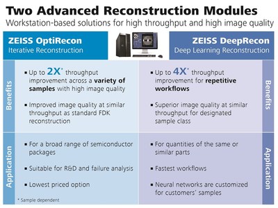
The new ZEISS Advanced Reconstruction Toolbox provides two new advanced reconstruction engines – OptiRecon and DeepRecon – that enable higher scanning speeds while maintaining or even increasing image quality with improved contrast-to-noise ratios for semiconductor advanced packaging failure and structural analysis. In addition to electronics and semiconductor packaging, the Advanced Reconstruction Toolbox can be used for myriad other applications, including materials research, life sciences and advanced battery development.
Professor. Dr. J.H. Shim of Dongshin University in South Korea, formerly a principal researcher in the electronics industry, stated, "Only ZEISS enables the visualization of the polymer separator in such a short scan time and with such a small number of projections. OptiRecon and DeepRecon are fantastic applications for industry battery customers."
OptiRecon for Diverse Samples and Workflows
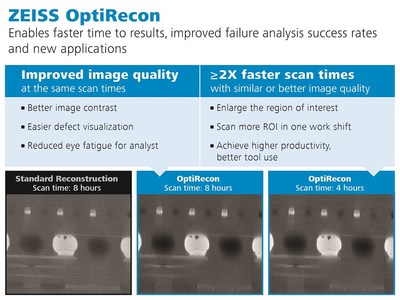
OptiRecon is ideal for a broad range of semiconductor packages and is suitable for both research and development applications, as well as FA. It uses a process known as iterative reconstruction, where differences are calculated between real and modeled projections through multiple iterations until convergence. OptiRecon enables optimal scan strategies using far fewer projections and less acquisition time compared to FDK. Up to two times faster scanning speeds with similar or better image quality can be achieved for semiconductor packages. This higher productivity enables multiple benefits: regions of interest can be enlarged, analysis jobs can be completed in a single work shift, and the sample's radiation dose can be reduced. At throughput levels similar to FDK, OptiRecon can provide improved image quality enabling better contrast-to-noise ratios, easier defect visualization and reduced eye fatigue for the analyst. It includes an easy-to-use interface to optimize reconstruction parameters and an advanced high-performance offline workstation for fast and efficient reconstruction.
DeepRecon for Repetitive Samples and Workflows
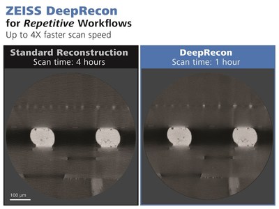
The DeepRecon module leverages custom-trained neural networks to enable higher throughput and higher success rates for FA and structural analysis applications requiring repetitive analysis of samples that are the same or similar to each other. ZEISS offers customized neural networks for specific sample classes that can be optimized to meet customer needs. Compared to FDK, DeepRecon enables scans up to four times faster with similar or better image quality for designated sample classes, as well as superior image quality with low noise when using the same scan time. Minimal effort is required to apply the desired DeepRecon network model for the workflow. The tool operator simply selects one of the ZEISS-developed network models from a drop-down menu.
"Since its introduction last year, the ZEISS Xradia 600-series Versa has seen strong momentum in the electronics and semiconductor packaging industry due to its superior resolution, image quality and throughput for package failure analysis," stated Dr. Stefan Preuss, head of ZEISS Process Control Solutions. "As our customers continue to face new challenges in advanced package failure analysis, ZEISS in turn is continually innovating to bring new capabilities and higher levels of performance to our products in order to meet those challenges head on. A case in point is our Advanced Reconstruction Toolbox with OptiRecon and DeepRecon modules, which provides a significant boost to throughput and image quality for these world-class imaging solutions – enabling our customers to accelerate their time to results and achieve higher package yields even more than before."
The ZEISS Advanced Reconstruction Toolbox with OptiRecon and DeepRecon modules is now available for upgrade on ZEISS Xradia Versa systems and ZEISS Xradia Context microCT systems, as well as future Versa and Context microCT systems.
For more information on the ZEISS Advanced Reconstruction Toolbox and other 3D X-ray imaging solutions from ZEISS, please visit: www.zeiss.com/pcs
About ZEISS
ZEISS is an internationally leading technology enterprise operating in the fields of optics and optoelectronics. In the previous fiscal year, the ZEISS Group generated annual revenue totaling more than 6.4 billion euros in its four segments Semiconductor Manufacturing Technology, Industrial Quality & Research, Medical Technology and Consumer Markets (status: 30 September 2019).
For its customers, ZEISS develops, produces and distributes highly innovative solutions for industrial metrology and quality assurance, microscopy solutions for the life sciences and materials research, and medical technology solutions for diagnostics and treatment in ophthalmology and microsurgery. The name ZEISS is also synonymous with the world's leading lithography optics, which are used by the chip industry to manufacture semiconductor components. There is global demand for trendsetting ZEISS brand products such as eyeglass lenses, camera lenses and binoculars.
With a portfolio aligned with future growth areas like digitalization, healthcare and Smart Production and a strong brand, ZEISS is shaping the future of technology and constantly advancing the world of optics and related fields with its solutions. The company's significant, sustainable investments in research and development lay the foundation for the success and continued expansion of ZEISS' technology and market leadership.
With over 31,000 employees, ZEISS is active globally in almost 50 countries with around 60 sales and service companies, 30 production sites and 25 development sites. Founded in 1846 in Jena, the company is headquartered in Oberkochen, Germany. The Carl Zeiss Foundation, one of the largest foundations in Germany committed to the promotion of science, is the sole owner of the holding company, Carl Zeiss AG.
Further information at www.zeiss.com
Semiconductor Manufacturing Technology
With its product portfolio and expertise, the Semiconductor Manufacturing Technology segment of ZEISS covers a variety of key processes in the production of microchips. Its products include semiconductor manufacturing optics – notably lithography optics – as well as photomask systems and process control solutions for semiconductor manufacturing. Thanks to ZEISS technology, microchips are becoming increasingly smaller, more powerful, more energy-efficient and more affordable. The electronic applications of these ongoing enhancements enable global progress in many disciplines such as technology, electronics, communication, entertainment, mobility and energy. Semiconductor Manufacturing Technology is headquartered in Oberkochen. Other sites include Jena, Rossdorf and Wetzlar in Germany, as well as Bar Lev (Israel) and Pleasanton, CA and Peabody, MA (USA).
![]() View original content to download multimedia:
http://www.prnewswire.com/news-releases/zeiss-adds-advanced-reconstruction-intelligence-to-3d-non-destructive-x-ray-imaging-for-improved-semiconductor-package-failure-analysis-301120673.html
View original content to download multimedia:
http://www.prnewswire.com/news-releases/zeiss-adds-advanced-reconstruction-intelligence-to-3d-non-destructive-x-ray-imaging-for-improved-semiconductor-package-failure-analysis-301120673.html
SOURCE ZEISS
| Contact: |
| Company Name: ZEISS
Victoria Doll, ZEISS Process Control Solutions, Email: Email Contact www.zeiss.com/newsroom Web: http://www.zeiss.com |


