Power considerations in sub-micron digital CMOS
2.5. Adders and computational power
Parallel multipliers are well known building blocks used in digital signal processors as well as in data processors and graphic accelerators. However, every multiplication can be replaced by shift and add operations. That is why, the adders are the most important building blocks used in DSP’s and microprocessors. The constraints they have to fulfill are area, power and speed. The adder cell is an elementary unit in multipliers and dividers. The aim of this section is to provide a method to find the computational power by starting from the type of adder. There are many types of adders but generally they can be divided in four main classes:
- Ripple carry adders (RCA);
- Carry select adders (CS);
- Carry look-ahead adders (CLA);
- Conditional sum adders (CSA).
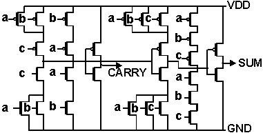
The starting point for any type of adder is a full-adder FA. An example of a full adder in CMOS is shown in fig.2.8. The discussion for this adder can be generalized for every type of adders. The outputs SUM and CARRY depend on the inputs a, b and c as:
![]() (2.18)
(2.18)
In a multiplier we are using parallel-series connections of full-adders to make a B bits adder with m inputs. In the following paragraph we make the assumption that every full-adder is loaded with another full-adder. Another assumption will be that the adder
|
|
|
Fig.2.8: Circuit diagram of a full adder FA |
has been optimized from the lay-out point of view to give minimal energies per transition when an input has been changed.
2.5.1. Ripple carry adders (RCA)
The reason to choose for ripple carry adders consists in their power efficiency [15] when compared to the other types of adders. Making an n bit ripple carry adder from 1 bit adders yields a propagation of the CARRY signal through the adder. Because the CARRY ripples through the stages, the SUM of the last bit is performed only when the CARRY of the previous section has been evaluated. Rippling will give extra power overhead and speed reduction but still, the RCA adders are the best in terms of power consumption.
In [15] a method to find the power dissipated by a B bits wide carry-ripple adder has been introduced. Denote Ea the mean value of the energy needed by the adder when the input a is constant and the other two inputs b and c are changed. This energy has been averaged after considering the transition diagram with all possible transitions of the variables. Eb and Ec are being defined in a similar way. Denote Eab the mean value of the energy needed by the full-adder when the two inputs a and b are kept constant and the input c is changing. By analogy we can define Eac and Ebc. The energy terms Ea, Eb, Ec and Eab, Eac, Ebc respectively depend on technology and the layout of the full-adder. Composing a m bits adder from a full-adder can be done in an iterative way as shown in fig.2.9. At a given moment, the inputs A[k] and B[k] are stable. After this moment every SUM output is being computed by taking into account the ripple through CARRY. The probability to get a transition on the CARRY output after the first full adder FA is �. After the second FA the conditional probability to have a transition is � and so on.
|
|
|
Fig.2.9: RCA m bits adder |
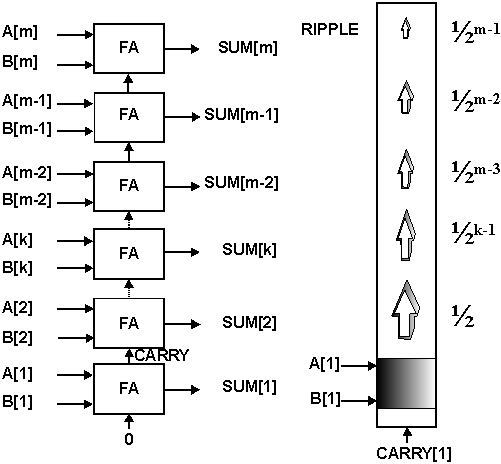
By using the same reasoning, the probability at the CARRY[m] is 1/2m-1. The inputs A[k] and B[k] are stable and we have to take into consideration only the energy Eab. For the first full-adder, when the inputs A[1] and B[1] are applied, the CARRY output is changing. The first adder contributes with Ec to the total energy. The bit k contributes with energy E[k] given by:
![]() (2.19)
(2.19)
The total energy dissipated by the m bits carry-ripple adder can be found by summing all contributions of the bits k. Hence, we get the total energy as a function of mean values of the basic energies of a full-adder FA:
![]() (2.20)
(2.20)
For large values of m eq.(2.20) can be approximated with the first term. This result can be used to compose cascade adders.
2.5.2. Cascade adders
To add m words of B bits length we can cascade adders of the type shown in fig.2.9. The result is illustrated in fig.2.10. We can assume statistical independence between the SUM and CARRY propagation in the following calculation. The SUM propagates in the direction l and the CARRY propagates in the direction k.
|
|
|
Fig.2.10: Cascade RCA for adding m words of B bits |
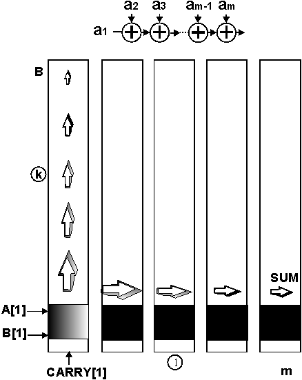
The energy needed for the SUM propagation is Eac and for the CARRY propagation Eab. Supplying the operands at the input b, the energy consumed at the bit (k,l) can be obtained from eq. (2.19):
 (2.21)
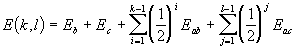
The total energy of the cascade adder is a sum of the energies needed by the individual bits and can be found by summing E(k,l) over k and l as shown in eq.(2.22).
![]() (2.22)
(2.22)
When the number of bits B equals the number of words m eq.(2.22) shows the dependence of power on the number of bits squared as explained earlier in the computational power. This shows how the total energy of the cascade adder can be related to the energy consumption of the basic building element, the full-adder FA. Now composing functions at higher level multiplication-like is possible.
2.5.3. Chain versus tree implementations of adders
In ripple through carry type of adders, a node can have multiple unwanted transitions in a single clock cycle before settling to its final value. Glitches increase the power consumption. For power-effective designs they have to be eliminated or, when this is not possible, at least limited in number. One of the most effective way of minimizing the number of glitches consists of balancing all signal paths in the circuit and reducing the logic depth. Fig.2.11 shows the tree and the chain implementation of an adder. For the chain circuit shown in fig.2.11(a) we have the following behavior. While adder 1 computes a1+a2, adder 2 computes (a1+a2)+a3 with the old value of a1+a2. After the new value of a1+a2 has been propagated through adder 1, adder2 recomputes the correct sum (a1+a2)+a3. Hence, a glitch originates at the output of adder 2 if there is a change in the value of a1+a2. At the output of adder 3 a worse situation may occur.
|
|
|
Fig.2.11: Chain (a) vs. tree (b) implementation of adders |
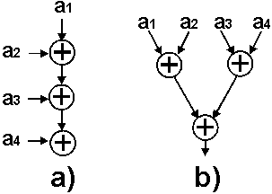
Generalizing for an N stage adder, it is easy to show that in the worst-case, the output will have N extra transitions and the total number of extra transitions for all N stages increases to N(N+1)/2. In reality, the transition activity due to glitching transitions will be less since the worst input pattern will occur infrequently. In the tree adder case shown in fig.2.11(b), paths are balanced; therefore the number of glitches is reduced.
In conclusion, by increasing the logic depth, the number of spurious transitions due to glitching increases. Decreasing the logic depth, the amount of glitches will be reduced, making possible to speed up the circuit and enabling some voltage down-scaling while the throughput is fixed. On the other hand, decreasing the logic depth, increases the number of registers required by the design, adding some extra power consumption due to registers. The choice of augmenting or reducing the logic depth of an architecture is based on a trade-off between the minimization of glitching power and the increase of power due to registers.