A 16-bit D/A interface with Sinc approximated semidigital reconstruction filter
7.7. Realization
The circuit diagram is illustrated in fig.7.19. The bitstream output of the noise shaper is applied to the DATA input terminal and shifted in the registers R1…R25. The outputs of the shift registers are applied to the AND gates AK. A return to zero signal RTZ derived from the clock CK is present at the other inputs of the AND gates and reduces the inter-symbol interference between the top flat current pulses. Therefore the signal dependent distortion is reduced. The coefficients of the filter a1...a25 are implemented as aspect ratios of the current sources connected transistors.
The switches are realized with differential pairs driven by the outputs of the AND gates AK and the outputs of the inverters IK. The output buffers of the AND gates and the inverters IK are chosen such that during transitions the switches are driven very fast in order to minimize the effects of the charge injection.
7.7.1 Floating current source
To minimize the mismatch between the pMOS and nMOS current sources, a floating mirror MN1 and MP1 delivers the same current IO to the pMOS and nMOS branches. The bias needed for cascoding is generated in the biasing section at nodes BIAS_N and BIAS_P. The floating current source is illustrated in fig.7.20. A replica of the bias current J_BIAS is forced in the transistor MN2. The same current is flowing in the transistor MP2. The MOS translinear loop around the transistors MN2, MP2 and MN1, MP1 generates a copy of the same current in the output transistors. An increase of the input current generates an increase of the voltage at the gates of MN2 and MN3. The feedback loop MN3, MN5 adjusts the current in the transistor MN5 to be equal with the current in the input branch. MN4 ensures a constant bias
|
|
|
Fig.7.20: The floating current source |
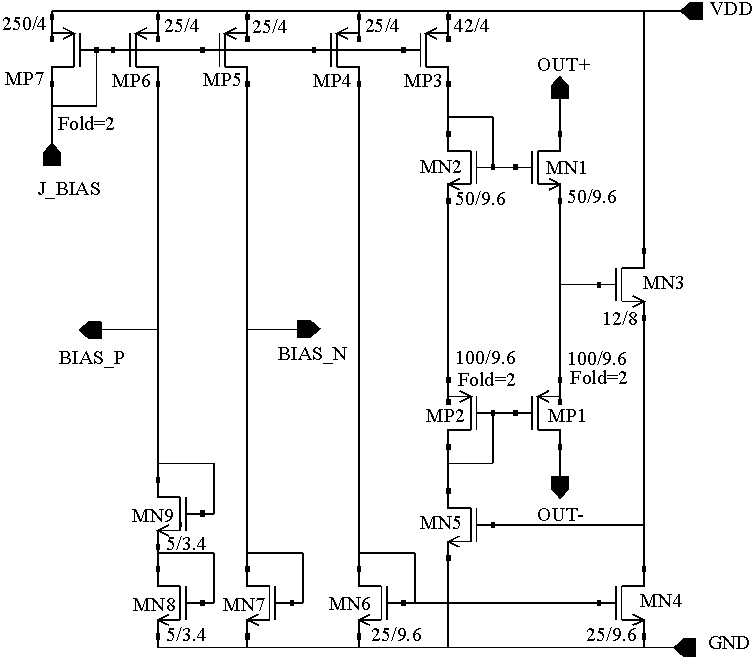
current in the transistor MN3. The outputs of the current source are floating and can withstand a minimum supply voltage of about 0.4V.
7.7.2 The opamp used for LPA filtering
The output of the D/A interface has to drive a high efficiency power amplifier with high linearity and low noise. Besides it has to deliver 1mA in a 10k differential load. The opamp of the RC-active low-pass filter is shown in Figure 7.21. It is a two stage Miller compensated opamp with a class A differential output. The first stage is a folded cascode amplifier with a large gain. The rail to rail output stage can deliver 1mA to the differential output load. Since a differential configuration is used, a common mode control circuit is required. The common mode at the output is sensed by resistors R1 and R2 and then applied at the inverting input of the differential pair MN16 and MN17 where it is compared to the reference voltage E_COMMON. The
|
|
|
Fig.7.21: The opamp used for LPA filtering |
|
|
|
Fig.7.22: The open loop gain of the opamp |
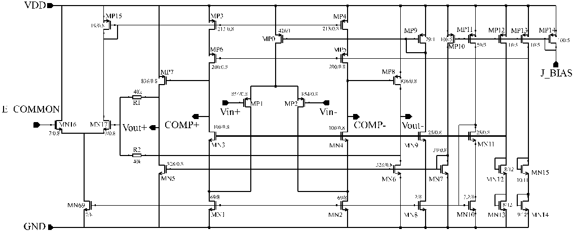
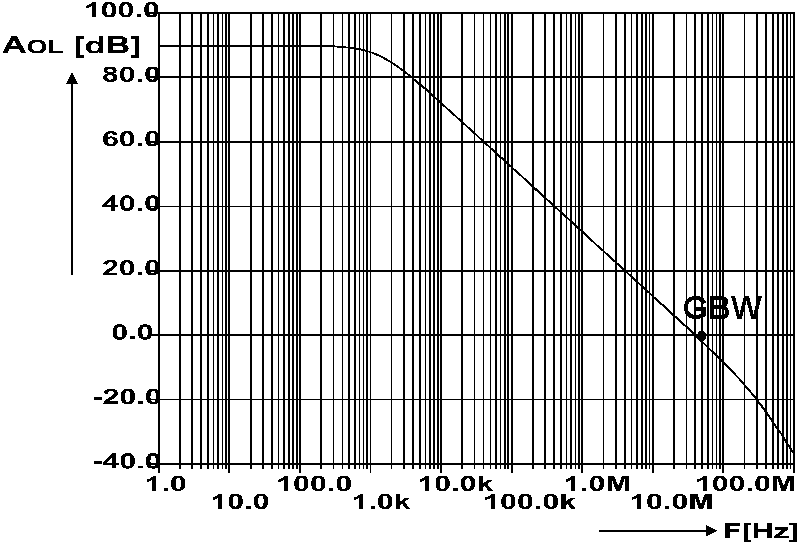
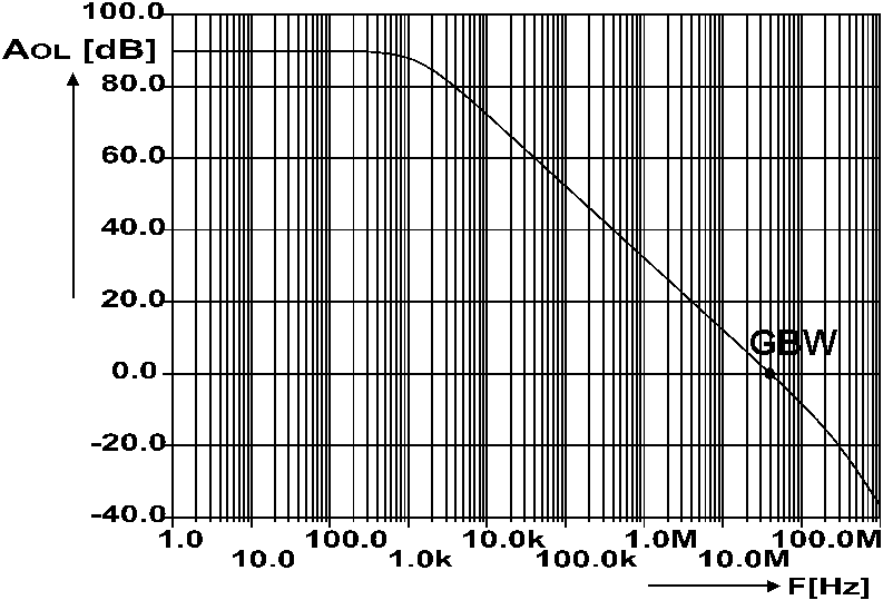
bias current of the first stage is adjusted in order to equalize the two voltages at the input of the sense amplifier. In fig.7.22, the frequency transfer of the amplifier is shown. The DC open loop gain of the amplifier is 90dB and the unity gain frequency 40MHz. The opamp is compensated with a Miller capacitor of 12pF in series with a resistor of 100W to correct for the phase shift introduced by the zero. This yields a phase margin of 75° . The noise behavior of the opamp is dominated by the noise of the first stage at low frequencies. The dynamic range of the amplifier is 103dB for a supply voltage of 5V. The power consumption of the opamp is dominated by the output stage power and has a value of 10mW from a 5V power supply voltage. In order to increase the dynamic range of the opamp for higher resolutions D/A interfaces, a class A chopped opamp can be used. Fig.7.23 shows a class A chopped amplifier based on the opamp from fig.7.21.
|
|
|
Fig.7.23: Class A chopped opamp |
|
|
|
Fig.7.24: The open loop gain of the class A chopped opamp |
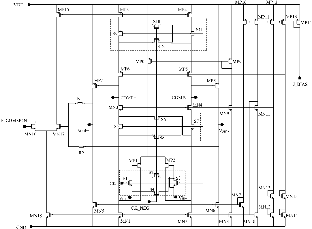
By introducing choppers S1..4 and S5...8 in the signal path (dotted lines) the stability of the opamp will be impaired. The chopper S9...12 matches dynamically the controlled current sources MP3 and MP4 outside the signal path. To improve stability, a larger compensation capacitor is required. The simulated frequency response of the opamp is shown in fig.7.24. The unity gain frequency is 17MHz, the phase margin has a value of 75° and the open loop gain is 90dB. For stability, a 14pF capacitor has been used in series with 320W .
7.7.3 Low-power D flip-flop for shift registers
The current sources of the FIR filter are controlled by switches driven from the outputs of a delay line as explained in section 7.4. The shift registers in the delay line are low-power D flip-flops realized with a minimum number of components as illustrated in fig.7.25. A master-slave action is required in order to isolate the output from the input. The D flip-flop consists of two inverters, two transmission gates and feedback to improve the switching behavior. When CK_NEG is active, the data D is loaded at the output of the first inverter and will be transferred to the output when CK
|
|
|
Fig.7.25: Low-power D flip-flop for shift registers |
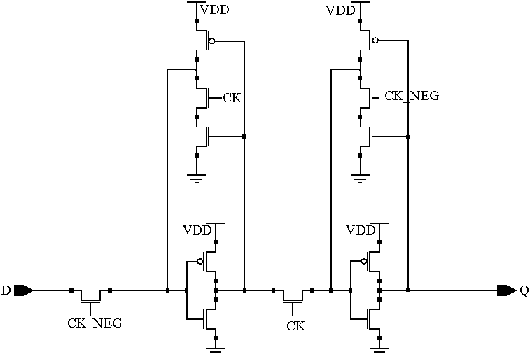
is active. By using simple transistors as transmission gates, the level "1" of the data D is degraded to VDD-VT. This slows down the low transition of the inverter. To correct this problem, a feedback path is added which restores the correct levels at the output. The main advantage of this approach is the reduction in the number of the clock lines and simplicity.