Power considerations in sub-micron digital CMOS
3.4. From fundamental limits to practical limits of power. Noise related power
The fundamental limits for low-power in analog are asymptotic limits without restrictions regarding topology, voltage swings, circuit topology, noise generated by active circuits, the process constants and linearity. Practical analog circuits show power dissipations of few orders of magnitude larger than fundamental limits. That is why it is important to know practical limits of circuits and to use them for comparing different possible solutions in order to make the right choice.
3.4.1. Noise prerequisites. Channel thermal noise
To make noise estimations we need the power spectral density of the drain current noise, valid for all possible working conditions of a transistor. The power spectral density of the current noise of a MOS transistor is proportional to the total charge stored in the channel, in the inversion layer |Qinv| [17]. This proportionality holds true for all working regions.
![]() (3.11)
(3.11)
GTH denotes the thermal noise conductance of the transistor. The thermal noise in most of the situations can be modeled either with a current source with a PSD of SI or with a voltage source with a PSD of SV as shown in fig.3.5.
|
|
|
Fig.3.5: Power spectral densities of the thermal noise |
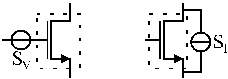
The value of Sv can be found from SI as a function of the thermal noise resistance of the transistor RTH.
![]() (3.12)
(3.12)
The value of the thermal noise conductance depends on the working region of the MOS transistor [17]. Table 3.2 gives the values of the thermal noise resistance RTH as a function of the slope factor n of a MOST and the working region of the MOST. Saturation denotes actually forward saturation in this case. Hence, a MOS transistor biased in triode region (strong inversion or weak inversion) will have a larger noise when compared to saturation noise. For a modern CMOS process the value of the slope factor n approaches unity and therefore, most of the noise models, agree that the
|
Strong inversion |
Weak inversion |
||||
|
triode |
saturation |
triode |
saturation |
||
|
GNTH |
ngm |
2ngm /3 |
ngm |
ngm/2 |
|
Table 3.2
: Thermal noise conductance of a MOSTpower spectral density of a MOST in strong inversion and saturation can be approximated with:
![]() (3.13)
(3.13)
3.4.2. Flicker
noiseBesides white noise we have additional low-frequency noise due to fluctuations of the density of charge carriers caused by trapping of the carriers in the oxide and in the neighborhood of Si-SiO2 interface. There are different theories but all agree over the dependency of the power spectral density of the noise on frequency and gate area as:
![]() (3.14)
(3.14)
where kF is a process dependent constant. Although 1/f noise is a low frequency random process, it appears also in RF CMOS circuits e.g. as phase noise in oscillators due to the nonlinear mechanisms which convert the low frequency noise in the side-bands of an oscillator, generating jitter. In older processes, the difference between the noise of a PMOST and an NMOST can be as high as 100 in the favor of PMOST’s. Modern processes without burried transistors show a smaller difference between the noise of a PMOST and a NMOST and an increase of 1/f noise spectral density. The advantage of using PMOS transistors for low noise properties is fading away as the process feature size shrinks. The problem of 1/f noise reduction techniques has been addressed in Chapter 5 and Chapter 6.
- Noise optimization through W- scaling of MOS transistor circuits.
Taking into account practical limitations it turns out that to preserve the dynamic range of analog circuits, the power dissipation has to increase when voltage supply is down-scaled. At low supply voltage it is important to have an optimization procedure for power [9]. Consider the following set of parameters important for a MOS transistor biased in saturation and strong inversion.
![]()
![]()
![]() (3.15)
(3.15)
![]()
![]()
First design a circuit to satisfy the DC and AC constraints and afterwards, for noise and offset considerations, scale up the widths of the transistors with a factor n, the lengths L are kept unchanged, the capacitances are scaled up a factor n, the resistors are scaled down with a factor n and the supply voltage is left unchanged. The time constants of the circuit are also not changed. As a consequence, the current in the devices will increase n times, the voltage drops on transistors and resistors remains the same but power, noise, offset and area will change. The power and the area are increasing with a factor n. The noise power spectral densities for the white and 1/f noise decreases a factor n and the offset decreases with a factor n [s2(Db/b) and s2(VT0)]. Therefore, improving the circuit for noise, there is an improve in matching as well. For current processing circuits, noise currents are more important and one has to refer to PSD of current noise and current matching of two transistors having the same drive voltage:
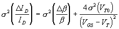 (3.16)
![]() (3.17)
(3.17)
Consequently, by W up-scaling, matching gets better but noise properties are getting worse. However, the DR for current processing increases with the same scaling factor n as long as the power of the signal increases with a factor n2 and the power of the noise with a factor n.
The W scaling is a method to travel along the analog limit for different S/N ratios. However it gives no clue whether the design is close to fundamental limits or not. For this, one should know how far away from the fundamental limits the actual design is. For optimal design, practical limits have to be considered for several alternative circuits. The strategy is to use the architecture which is closer to the fundamental limits. Once the best circuit is known, scaling the design according to W scaling allows to find the best trade-off between power, speed and dynamic range to fit the specifications of the design.
3.4.4. Noise driven power consumption for elementary stages
Power estimations based on the simple model described above are far away from the actual power consumption of analog circuits. The forthcoming section presents a general theory for power consumption of elementary stages based on noise and accuracy. Optimal design from power point of view is being discussed which provides the background for implications of noise and mismatch on the performance of analog systems.
3.4.5. Voltage processing circuits
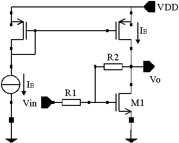
One of the basic voltage processing stages is the inverting amplifier shown in fig.3.6. The closed loop gain of the circuit is determined by ratios of resistors well controlled over process variations. The frequency response of the amplifier is given below:
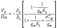
Considering the transconductance of the transistor M1 larger than 1/R1 and 1/R2, the low frequency loop gain is defined only by the ratio R2/R1. In this case, the power spectral density of the output noise can be found from the input power spectral density and the gain G=R2/R1. The noise generated by PMOS transistors can be neglected for large gains G.
![]()
Here, we can assume a negligible contribution of the white noise generated by the resistors compared to the noise generated by the transistor e.g. choosing large values for G and small values for R1. Denote BW the bandwidth of the amplifier BW=gm/2pCgs. The noise power at the output can be determined by using the noise bandwidth approach:
|
|
|
Fig.3.6: Voltage amplifier with feedback |
![]() (3.20)
(3.20)
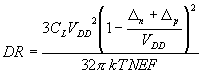
The voltage swing is limited by the saturation voltages Dp=|VGT,p| and Dn=VGT,n of the PMOS and NMOS transistors to VDD-Dn-Dp. The dynamic range at the output is found by dividing the power of the signal [(VDD-Dn-Dp)/2Ö 2]2 to the noise power:
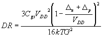 (3.21)
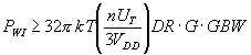
In conclusion, the DR of the stage decreases for low power supply voltages and for large gains. When VDD > > Dn+Dp the term in parenthesis can be approximated with one. At low supply voltage it is a second order effect decreasing further the DR. By multiplication of DR with G*GBW and using gm=2IB/(VGS-VT) we get:
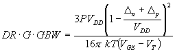 (3.22)
In eq.(3.22) P is the power needed to bias the gain stage P=IBVDD. The total performance of the amplifier is only dependent on the chosen bias point of the stage, some technology constants and is independent of transistor sizes. In a voltage processing stage, VDD and VGS-VT can be chosen independently as long as the supply limits are not trespassed. The total performance of the amplifier can be maximized by lowering VGS-VT. This corresponds also with the requirements to get low offsets as it will be explained in section 3.5. The minimal value of VGS-VT in the saturation region is the saturation onset, such that VGT@ 2nUT [Wassenaar] where UT represents the thermal voltage. Accordingly, (3.22) becomes:
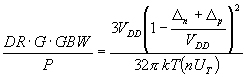 (3.23)
This ratio can be considered as a figure of merit for this stage where all important design parameters are present. The required power consumption will be fixed for a given dynamic range, gain and gain-bandwidth. Therefore, the minimal power consumption of this stage biased in strong inversion when VDD > > Dn+Dp is:
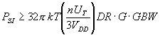 (3.24)
When biasing the stage in weak-inversion gm=IB/(nUT), the transconductance remains the same and the minimum power consumption for the same requirements is:
 (3.25)
In both situations decreasing the power supply voltage, power will increase while keeping the same DR*G*GBW product.
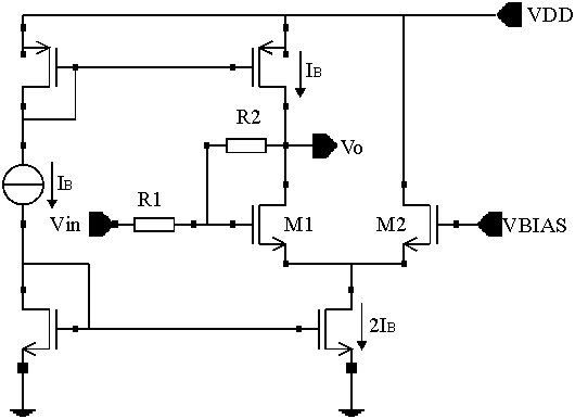
Fig.3.7 shows a voltage amplifier with differential stage and feedback. To make the gain at low frequencies dependent only of the ratio of the two resistors, the transconductance of the transistors M1 and M2 should be made larger than 1/R1 and 1/R2. Due to the single ended output and doubling of the input noise spectral density, the trade-off between DR and G*GBW is found to be (VGT@ 2nUT):
 (3.26)
Consequently, the minimal power consumption of this stage biased in strong inversion will be:
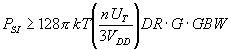 (3.27)
The power consumption compared to the single transistor voltage amplifier has been increased four times. The efficiency of this stage is worsened due to the single ended output and differential input. This adds extra noise without the possibility of having large swings like in a differential output case. Minimal power in weak-inversion will be the same:
|
|
|
Fig.3.7: Voltage amplifier with differential stage and feedback |
 (3.28)
Fig.3.8 shows an operational transconductance amplifier (OTA) with differential stage and active load. This OTA is commonly used in many designs involving operational amplifiers. It also appears in some of the designs from the next chapters. Assume that OTA has been configured as a follower and the load capacitance at the output is CL. The GBW product of the stage depends on the transconductance of the input stage and the load capacitance CL. For accuracy reasons the input stage has been biased in weak-inversion. The GBW of the OTA is:
![]() (3.29)
(3.29)
The power spectral density of the input voltage noise can be found from:
 (3.30)
where NEF represents the noise excess factor. For low noise, the transconductance of the input pair has to be larger than the transconductance of the active load. The noise excess factor NEF is close to unity in this situation. The DR at the output in a follower configuration is:
 (3.31)
|
|
|
Fig.3.8: OTA with active load |
The product DR*GBW does not depend in this case on VGT due to the weak inversion biasing of the input transistors. As a minimum limit of power for the OTA in a follower configuration (G=1) we have:
 (3.32)
The same result holds true for strong inversion. A robust design of the OTA requires phase margins larger than 45° . The second pole of the OTA can be found from:
 (3.33)
The phase margin condition requires a value for f2 of about f2 ³ 2GBW and that is why we can still use the equivalent bandwidth approach. When comparing the OTA case with G=1 and the case in fig.3.7 it seems that minimum power consumption in both cases is the same. However, in the OTA case configured as a follower the distortion is higher due to the lack of a rail to rail input. The voltage swing will be lower for the same harmonic distortion. That is why, the power efficiency of the OTA configured as a follower is worse when compared to inverting amplifier from fig.3.7 with G=-1.
Fig.3.9 shows a feedback amplifier with an OTA. If G denotes the low frequency gain of the amplifier, the gain-bandwidth product of the amplifier can be found from the input transconductance gm,in and the output load capacitance CL. The input stage is biased in weak inversion with a current source II. Denote h =II/ITOT the current efficiency of the input stage and ITOT the total current needed to bias the opamp. The gain-bandwidth product GBW is:
![]() (3.34)
(3.34)
|
|
|
Fig.3.9: Feedback amplifier with OTA |

Following the same pattern like in the previous case, the minimum power needed to bias this amplifier is found to be:
 (3.35)
The higher the power efficiency of the input stage, the lower the power coonsumption. When G=1 and h =1 this circuit degenerates in the previous case.
3.4.6. Current processing circuits
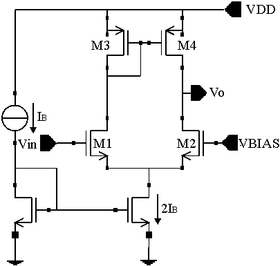
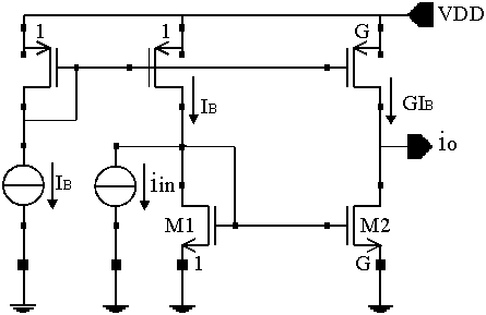
Consider the basic current amplifier from fig.3.10. The input current iin is amplified with a factor G by the output transistor M2. The gain G is set by aspect ratios without the need for large output resistance transistors. The transfer of the current amplifier shows the presence of a zero at high frequencies due to feed-forward capacitor Cgd2 and a pole:
![]() (3.36)
(3.36)
The pole of the amplifier is determined by the capacitance C1=Cgs1+Cgs2 by neglecting other capacitances present at the input node. Fig.3.11 shows the frequency transfer of the current amplifier. The gain G at low frequency depends only on aspect ratios. Tuning the current IB, the dominant pole and the zero shifts along the frequency axis keeping the same relation between the first pole, GBW and the zero. Therefore, it is possible to change the GBW of the amplifier without changing the gain. The product G*GBW is not constant like in the case of voltage amplifiers [18]. In the case of a large gain G, the noise at the input is determined only by the transistor M1 and the PMOS current source. Assuming that the mobility factor of the carriers of a NMOS is 3 times larger than the mobility factor of the carriers in a PMOS, the power spectral density of the noise related to the input is:
|
|
|
Fig.3.10: Current amplifier |
|
|
|
Fig.3.11: Frequency transfer of the current amplifier |
 (3.37)
Within the assumption that white noise is dominant and the zero positioned at high frequency, the output power spectral density and output noise can be determined from:
 (3.38)
The noise power can be found from the noise power spectral density SIout by integration over the positive frequencies or by using the noise bandwidth approach:
 (3.39)
Hence, one can find the dynamic range at the output of the current amplifier, defined as the ratio between the power of the signal current and the power of the noise current.
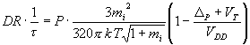
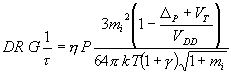
The transistors M1 and M2 are biased in strong inversion. If a current modulation index mi is considered such that distortions are sufficiently low, then the DR is:
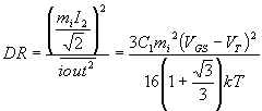 (3.40)
For any type of current processing circuits the power supply voltage VDD and the gate drive voltage cannot be chosen independently. Increasing the input current, the gate voltage of M1 is pulled up and at maximum will reach the voltage VDD-Dp where Dp is the saturation limit of the PMOS current source transistor. Now, we can relate the quiescent gate drive voltage to the maximum value limited by the supply:
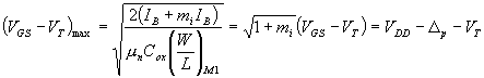 (3.41)
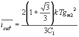
The extra constraint from (3.41) shows that VDD and VGS-VT cannot be chosen independently for this case. The dynamic range can be rewritten as a function of the supply voltage:
 (3.42)
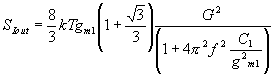
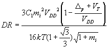
Therefore, the lower the supply voltage, the lower the DR of the amplifier. The DR can be increased by increasing the capacitance C1 and/or the modulation index mi. The term containing VDD at denominator can be regarded as a second order effect meant to decrease the DR for low supply voltages. For large gain factors G, the bias power P=(G+1)IBVDD can be approximated with GIBVDD and the factor of merit for this amplifier will be:
 (3.43)
As a second order effect, at low supply voltages VDD@ DP+VT the efficiency of the current amplifier decreases and we need to use more power in order to keep the same DR*GBW product as explained below:
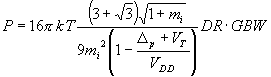 (3.44)
The different performance specifications of a current amplifier like DR, GBW and power are linked and depend on technological and physical constants. This simply shows that in current or voltage mode circuits one cannot get high DR at high speed without paying in additional power. The designer cannot choose the different performance specifications independently. A special case is the W scaling. By W scaling the circuit, the DR increases at the expense of power but keeping the GBW of the amplifier constant. The same methodology can be applied for other current-mode circuits [33], [34], [35], [36], [37].
3.4.7. Sampled data applications
The results obtained in the previous section can be generalized to sampled data circuits. Sampled data analog circuits like switched-capacitors and switched-currents are subject to the same trade-off found in continuous time circuits.
3.4.7.1. Switched-capacitors charge summing amplifier
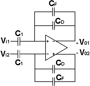
One of the most general configurations in switched-capacitors circuits is the charge summing amplifier with sample and hold amplifier at the output illustrated in fig.3.12. The results obtained for this amplifier can be used for switched-capacitor integrators. The amplifier is actually a differential OTA with common-mode control. A simple analysis shows the low-pass character of the amplifier and the S/H circuit. Denote qin the input charge, fS=1/T the sampling frequency and V0 the output differential voltage of the first amplifier. For two clock cycles 1 and 2, the output of the first amplifier represents an amplified version of the input charge with a low-pass character:
 (3.45)
The second amplifier is a S/H amplifier with a low-pass effect on the output of the first amplifier. If VS denotes the differential voltage at the output of the S/H, then:
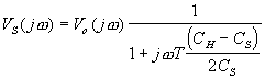 (3.46)
|
|
|
Fig.3.12: Charge summing amplifier with S/H |
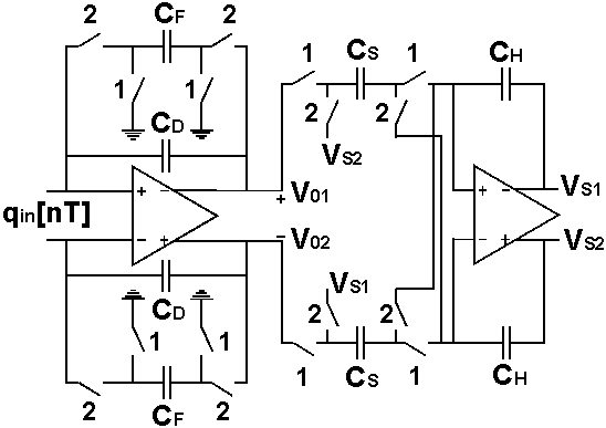
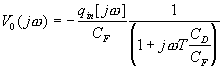
To simplify our discussion, consider only the charge amplifier with input capacitances C1 and the simplified switching approach as shown in fig.3.13. The reference voltage VREF has a value of VDD/2. The main sources of noise are discussed in the following section.
a. Switch noise
Every switch in the configuration has a finite on resistance which generates white noise. This wide-band noise is being sampled on the corresponding capacitor which limits also the noise bandwidth. The two-sided power spectral density of the voltage noise sampled on the capacitor C1 is [19], [20]:
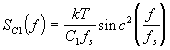 (3.47)
After low pass filtering in a bandwidth fsig, the baseband, the noise power of the sampled switch noise has a value of:
![]() (3.48)
(3.48)
This noise sampled on C1 is amplified to the output of the amplifier:
 (3.49)
|
|
|
Fig.3.13: Switched capacitor amplifier |

The contributions of the other switches can be neglected compared to the above noise contribution.
b. Noise of the OTA
At the output of the first OTA we have two noise components due to the equivalent noise voltage "seen" at the input of the OTA. There is a direct noise component at the output transferred by the low frequency gain (1+G). Another noise component comes from the thermal noise of the OTA folded back into the baseband due to undersampling of the input capacitor C1.
- Direct noise
If the thermal noise is band limited at the output to fsig the direct component of the thermal noise generated by the OTA has a power of:
![]() (3.50)
(3.50)
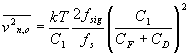
- Undersampled noise
The thermal noise component of the OTA is bandlimited by the OTA. The sample frequency is lower than the GBW frequency of the OTA for settling considerations. For fast settling we need undersampling factors 2fGBW/fs of about 10. Therefore, the extra white noise bands are increasing the baseband noise with a factor 10 by folding back the thermal noise.
![]() (3.51)
(3.51)
This is the largest noise component existent at the output of the OTA. Compare now the folded back noise to the switch noise. Given the values of the capacitor C1 in pF range and the value of the input transconductance of the OTA in order of few hundreds of m S it is the folded noise which dominates over the switch noise from (3.51). The noise and power analysis from reference [21], considered as a reference for switched-capacitor circuits has ignored the folded back component of the noise. Compared to the continuous time case, the extra undersampling factor 2fGBW/fS increases noise. The settling requirement makes the noise properties of the switched capacitor worse when compared to the continuous time approach. The S/H amplifier has an output noise which can be found from (3.51) when G=1 (CH=CS). Hence, the theoretical transfer function of the S/H becomes unity and the same procedure can be applied for it.
c. Settling time
As an intermediate step towards power computation, the settling time of the switched-capacitor amplifier is being determined from fig.3.14. The settling time can be found from the feedback factor of the amplifier and the unity gain frequency. From fig.3.14 the feedback factor of the amplifier is found:
|
|
|
Fig.3.14: Circuit for settling time computation |
![]() (3.52)
(3.52)
Given the transconductance of the input stage gm the unity gain frequency is:
![]() (3.53)
(3.53)
Denote h the current efficiency of the input stage. From (3.52) and (3.53) we can find the theoretical settling time constant as:
![]() (3.54)
(3.54)
The input stage of the OTA has been biased in weak inversion. In sampled data circuits the power trade-off involves 1/t instead of GBW. Considering only the undersampled noise from (3.51) the trade-off is:
 (3.55)
At limit fs=2fsig which is valid also for switched capacitors filters based on bilinear transformation. The minimum power of the SC amplifier is found from (3.55):
 (3.56)
It is not surprising to discover the resemblance between (3.56) and (3.35) which makes the connection between sampled data circuits and continuous time circuits.
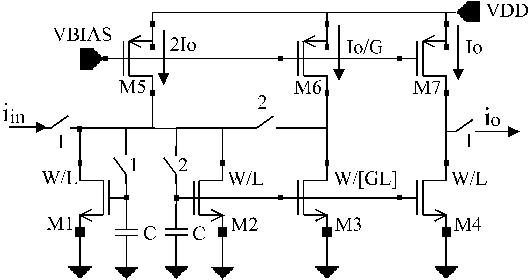
3.4.7.2. Switched-currents applications
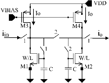
The memory cell from fig.3.15 is the basic element in switched currents amplifiers, delay elements and integrators [22], [23]. For simplicity, assume a first order behavior of the memory cell. The theoretical settling time constant is C/gm where gm represents the transconductance of the memory transistor. For settling reasons, the time constant C/gm should be about ten times larger than the Nyquist sampling period. At the end of phase 1, the voltage across the capacitor C is stored together with a noise voltage and a voltage error due to the charge injection from the switch. The noise on the capacitor C is due to the intrinsic noise of M1 and the noise generated by the switch ON resistance. The noise variance on the capacitor generated by the noise current source of M1 is 2kT/3C given the noise bandwidth approximation. This noise on the gate of M1 gives an output current noise with variance:
![]() (3.57)
(3.57)
This noise is sampled again on the gate of M2 and gives a noise voltage on the transistor M2 with a variance of 2kT/3C. The total voltage noise variance on the gate of M2 will be 4kT/3C which generates at the output of M2, a current noise with a power of:
![]() (3.58)
(3.58)
Given the undersampling effects on the capacitor C the noise will be increased with a factor 2GBW/fs [19] and therefore the dominant noise component it is not the direct noise of the transistors but the undersampled noise. Settling reasons impose an undersampling factor of about 10 and the folded noise in the baseband is:
|
|
|
Fig.3.15: SI memory cell |
![]() (3.59)
(3.59)
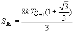
Given the modulation index mi, the saturation limit Dp of the current source I0 and using again eq.(3.41) we get:
 (3.60)
The minimum power consumption of the memory cell can be found by neglecting the last term from (3.60):
 (3.61)
The power efficiency of the SI memory cell is low when compared to continuous time current amplifier. The band-limiting action for the noise is performed here only by memory capacitor C. That is why the noise is integrated in a large bandwidth which gives a large amount of noise. The SI memory cell can be used to generate a large class of switched current circuits like amplifiers, integrators and delay cells [24], [25], [26]. Fig.3.16 shows a possible application of the memory cell, a SI amplifier (lossy integrator). Although this integrator suffers from charge injection it can be used as an example to illustrate our theory. The damped integrator contains an extra feedback stage M3 weighted with a factor 1/G where G represents the low frequency gain of the amplifier/damped integrator. To understand the behavior of the circuit we have to consider the currents through the transistors M1 and M2 in the clock cycles f 1 and f 2:
![]() (3.62)
(3.62)
![]() (3.63)
(3.63)
|
|
|
Fig.3.16: SI non-inverting amplifier (damped integrator) |
During the phase f2 the relationship between the output current and I2 is:
![]() (3.64)
(3.64)
Hence, the transfer function of the circuit is found from the Z-transform of (3.62), (3.63) and (3.64):
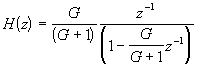 (3.65)
By multiplying the denominator and the numerator of H(z) with z1/2 under the low frequency approximation ejwT@ 1+jwT, the transfer function and the cuttof frequency of the amplifier are:
 (3.66)
If the ratio between the transconductances of the NMOS transistors and their PMOS biasing counterparts is g and the transconductance of the transistors M1 and M2 is gm, the current noise PSD related to the input is found to be:
![]() (3.67)
(3.67)
The noise bandwidth is p/2 larger than fLP and the power of the noise at the output due to fold-over effects is found from (3.67) the transfer function and the undersampling ratio. The quiescent value of VGS-VT cannot be chosen independently of supply. Given the settling time t=2pC/gm, the current efficiency of the amplifier h and using (3.41) we have:
 (3.68)
The minimal power consumption of the switched-currents amplifier is found when VDD>>DP+VT:
 (3.69)
- Power consumption and power supply voltage down scaling
From previous section appears that scaling down the supply voltage, power has to increase in order to keep the same performances. The question is if there are circuits less sensitive to VDD down scaling. In order to answer this question consider the power consumption for a voltage or current-mode circuit either continuous time or sampled data.
![]() (3.70.a)
(3.70.a)
![]() (3.70.b)
(3.70.b)
Scaling down VDD, in order to keep the same DR*GBW product, power has to increase faster in voltage-mode circuits to compensate for power supply down scaling. The explanation for this result comes from the nonlinear relationship between voltages and currents in a current mode circuit whereas in voltage-mode circuits the relationship is linear [see eq.(3.41)]. Similar conclusions will be found in the next paragraph.