Low-noise, low residual offset, chopped amplifiers for high-end applications
6.4. A low noise, low residual offset, chopped amplifier in 0.8
mm CMOSAs already mentioned, the opamp consists of a gain stage and an class AB output stage. Driving a low ohmic load of 32W with a rail to rail output, the opamp has to deliver some 160mA to the load. To reduce power consumption, a class AB output stage is therefore needed. This section presents a low noise, low residual offset, chopped amplifier with a class AB output stage [7] in 0.8mm CMOS technology.
6.4.1. The class AB control circuit
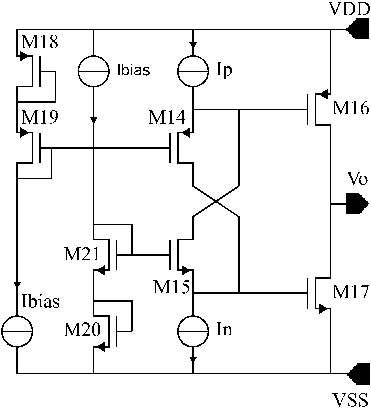
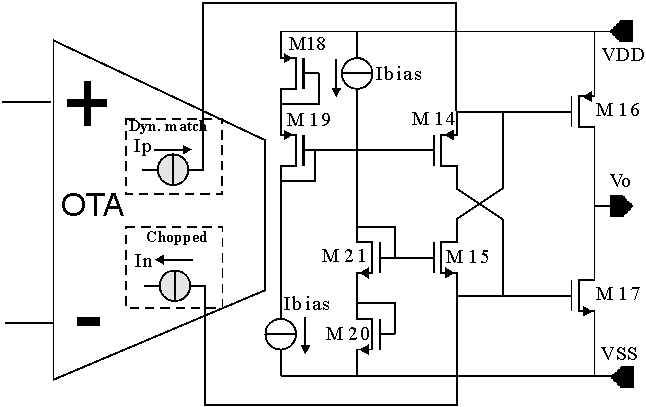
There are many different ways to construct a class AB control circuit. The circuit shown in fig.6.7 combines simplicity and good stability properties [8]. The principle of operation is based on two MOS translinear loops M14, M16, M18, M19 and M15, M17, M20, M21 respectively. The quiescent current in the output transistors is controlled by the two loops. In steady state, with no signal at the input, the currents In and Ip are equal and they are equally divided between M14 and M16. The bias current Ibias ensures a constant voltage at the gates of M14 and M16. Therefore a
constant bias current flows through M16 and M17. The presence of the signal in the current In determines an imbalance between the currents In and Ip and the currents flowing through M14 and M15 are not equally divided. This gives a change in the currents flowing in M16 and M17 generating a current flowing into the load. There is always a minimum current Imin flowing in the output stage and the output transistors are never turned off. The minimum current is determined by Ibias and some aspect ratios. Denote Iq the quiescent current in the output transistors and assume In=Ip=2Ibias in steady state. Consider the two MOS translinear loops M14, M16, M18, M19 and M15, M17, M20, M21 respectively under the conditions (W/L)14=(W/L)19 and (W/L)15=(W/L)21. Then, the relationship between the quiescent current and the bias current is found from:
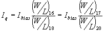 (6.1)
(6.1)
If Imin denotes the minimum current allowed in the output transistors, then the relationship between Iq and the minimum current is:
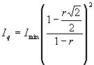 (6.2)
(6.2)
|
|
|
Fig.6.7: The class AB control circuit |
The factor r depends on the aspect ratios of the transistors in the translinear loop and holds for NMOS as well for the PMOS counterparts M15, M20, M21 and M14, M18, M19 respectively:
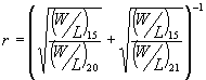 (6.3)
(6.3)
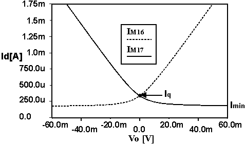
Fig. 6.8 shows the simulation of the class AB currents in the output transistors as a function of the voltage across the load (RL=32W ). The quiescent current has been taken Iq=300mA.
6.4.2. The circuit principle
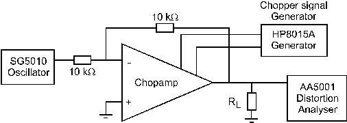
The principle of the opamp is based on the circuit shown in fig.6.9. It is explicitly shown that the output stage and the OTA share the same current which can be chopped according to the principle illustrated in fig.6.5.c. The In current delivered by the OTA is chopped while the current Ip delivered in top will be dynamically matched to eliminate its offset. By sharing the same bias some of the offset generated by the class AB output stage is eliminated. The remaining offset is generated by the currents Ibias.
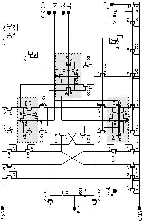
In fig.6.11, the complete circuit diagram of the opamp is shown. The input chopper M30, M31, M32 and M33 transposes the differential input signal applied to the Plus and Min terminals to the alternate output nodes of the modulator. As a result, the input signal is modulated at odd harmonics of the chopper frequency. The second chopper M34, M35, M36 and M37 demodulates back the signal and modulates 1/f noise and offset at odd harmonics. In order to cancel out the noise and offset of M8 and M9, the third chopper M38, M39, M40 and M41 matches dynamically the two branches. A low voltage cascoded mirror M3, M4, M5 and M6 performs a differential
|
|
|
Fig.6.8: The class AB currents in the output transistors |
|
|
|
Fig.6.9: The circuit principle |
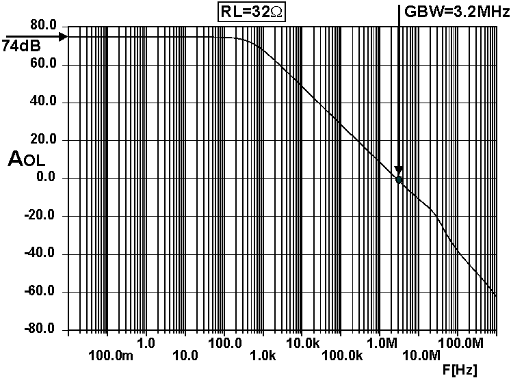
to single ended conversion for the signal which is applied to the output stage. The class AB output stage uses two MOS translinear loops to control the current in the output transistors. The offset of the output stage is mainly caused by mismatch between the currents of M22 and M26. In fig.6.10 the simulated transfer of the opamp loaded with 32W is presented. The open loop gain is 74dB and the phase margin is 81° for a GBW of 3.2MHz. The quiescent current of the output stage has been chosen Iq=300mA for linearity reasons. The output transistors have large dimensions and can deliver 160mA short circuit current in a rail to rail configuration without latching.
|
|
|
Fig.6.10: The frequency transfer of the opamp |
|
|
|
Fig.6.11: The circuit diagram |
6.4.3. Measurements
The chopped amplifier has been realized in a 0.8m m CMOS digital technology with one polysilicon layer and two metal layers. Special layout techniques have been used to reduce the mismatch and charge injection of the switches. Ten arbitrarily chosen samples, have been measured. The two complementary chopper signals are generated by a pulse generator with complementary outputs and adjustable rise and fall times. The connections to the testing board are made with 50W BNC-SMD coax cable 50W terminated to reduce reflections. A bias current of 30mA is used to bias the amplifier.
a. Noise measurements
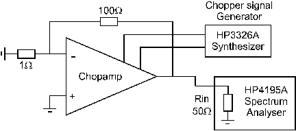
In order to verify the reduction of 1/f noise in the baseband, a spectrum analyzer measures the spectrum of the amplifier configured as an amplifier with 40dB gain as depicted in fig.6.12. The reason was the noise floor of the analyzer, higher than the noise of the opamp. The two resistors give negligible contributions to the total noise. At the output, the spectrum analyzer measures the noise of the amplifier amplified with 40dB in a bandwidth of about 100KHz which is exactly the bandwidth of the low pass filter in the D/A interface.
|
|
|
Fig.6.12: Noise measurement setup |
A HP-VEE program has been used to make possible time averaging of measurements. The measurements have been done with different chopping frequencies and different rise and fall times. In fig.6.13, the output noise spectrum is shown. The chopping frequency is 1MHz, situation showing the reduction of 1/f noise. At input, the residual noise is the white noise of the amplifier, attenuated with about 3dB compared to the unchopped case.
The rise and fall times of the chopper modulator have an important effect on the reduction of 1/f noise. The larger the transition times, the more important becomes the 1/f noise from the switches which have small dimensions and inherently large noise. In fig.6.13 the rise and fall times of the chopper signals are 5ns. Chopping at 10MHz, the influence of the transition times on the chopper signals becomes important and the 1/f noise is not reduced completely with transition times in the interval tr=10ns…20ns. However, chopping at 10MHz with tr=5ns the 1/f noise can be
|
|
|
Fig.6.13: The output spectrum of the opamp |
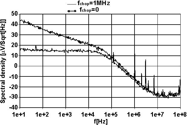
completely removed. The residual thermal noise at the output of the opamp is about 5dB[mV/Ö Hz] and the input noise of the opamp 40dB less. When the load resistance is 32W , the maximum output voltage is 2.6Vpp. The dynamic range of the amplifier configured as a follower in audioband is 111dB when chopping at 1MHz. The S/N+THD figure (SINAD) is about 10dB lower due to distortion reasons.
b. Offset measurements
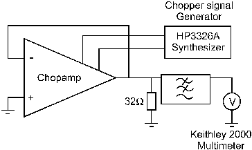
The amplifier has been configured as a follower for offset measurements. The static offset can be measured directly at the output. For dynamic measurements the output is low pass filtered and a digital mVolt-meter measures the output offset as illustrated in fig.6.14. Ideally only the offset of the output stage should remain but, second order effects like mismatch of the switches and non-ideal behavior of the
|
|
|
Fig.6.14: Static and residual offset measurement setup |
|
|
|
Fig.6.15: Residual offset vs. chopper frequency |
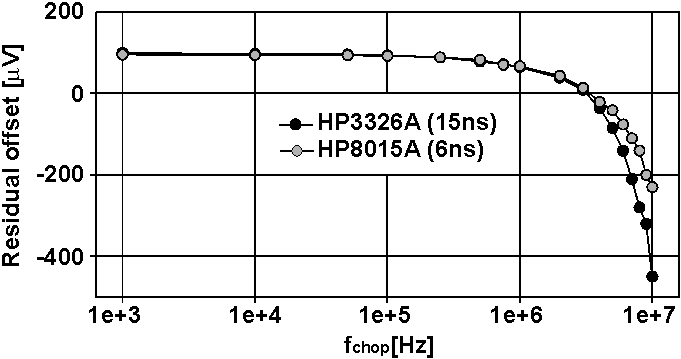
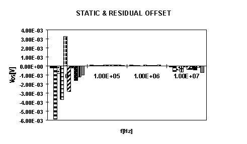
chopper signals are the cause of the residual offset when the chopper frequency increases. The measured static offset has a mean value of 1.7mV with a standard deviation s =2.5mV. For the measurement, ten arbitrarily chosen samples have been considered. When choppers are activated, the measured residual offset can be plotted as a function of chopper frequency. This is shown in fig.6.15. The two graphs correspond to different transition times generated from two different pulse generators. The upper curve corresponds to a 6ns transition time and the lower curve corresponds to 15ns transition time. Up to 8MHz, the residual offset is lower than 100m V. This is mainly generated by the output stage. In this frequency range, the transition time of the chopper signal is not important. The residual offset is virtually independent of a change in rise or fall time. This shows again that offset can be treated just as low frequency noise. At higher frequencies, the larger the transition time, the higher the offset. Fig.6.16 shows the offset of the ten samples at different chopping frequencies.
|
|
|
Fig.6.16: Static and residual offset measurement setup |
|
|
|
Fig.6.17: Distortion measurement setup |
c. Linearity measurements
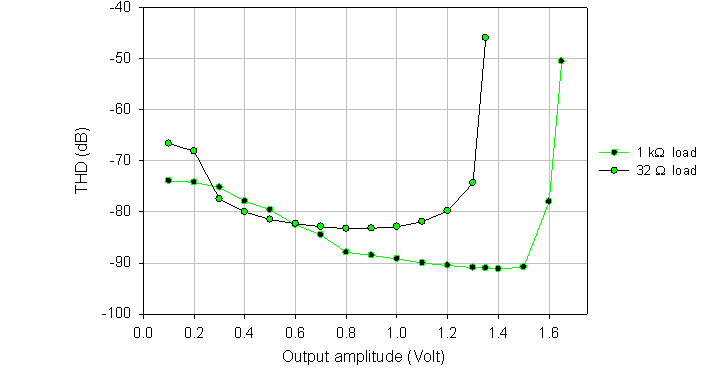
The linearity measurement setup is presented in fig.6.17. The THD of the opamp was measured as a function of amplitude and frequency. The input sine-wave has been supplied by a low distortion oscillator. THD of the input signal is -90dB which determines the lower limit of the measurable distortion. The THD is independent of the chopper frequency and that is why all linearity measurements have been done with 1MHz chopper frequency. To use the full swing at the output the amplifier has been configured as an inverting amplifier with 0dB gain. The linearity measurement versus amplitude at 1KHz is illustrated in fig.6.18. When the load is 32W , clipping occurs at 1.35V output amplitude. With 1kW load, clipping occurs close to the supply voltage at 1.65V output amplitude. The lowest input signal handled by the the distortion analyzer is 60mV an that is why the THD is not measured at lower amplitudes. For high ohmic loads, the THD is better than -91dB for 1.5V voltage swing. For low ohmic loads, the THD is better than -83dB. The linearity at low amplitudes is impaired by cross-over distortion.
|
|
|
Fig.6.18: THD vs. output amplitude |
|
|
|
Fig.6.19: THD vs. output frequency |
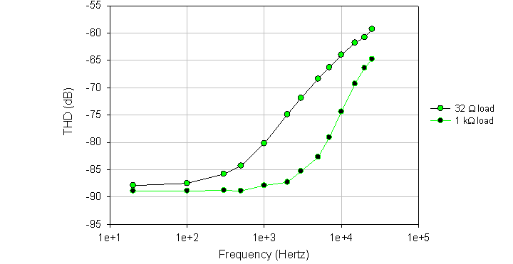
With high ohmic loads, the linearity of the amplifier is better because the output stage has a higher gain and does not have to deliver large currents to the load. The linearity depends on the quiescent current flowing in the output transistors. The current consumption of the opamp is mostly determined by the quiescent current in the output stage. For the measurements Iq has a value of 300m A. The THD as a function of frequency is illustrated in fig.6.17. It was measured in the audio band with two different loads. The output signal amplitude is 0.8V. The linearity with a 1kW load at 1KHz is better than -88dB and -80dB for a 32W load. At high frequencies, the loop gain falls and the effect of the feedback becomes less effective. The complete summary of performance is shown in Table 6.1.
|
PARAMETER |
VALUE |
|
Technology |
0.8m m, 1PS, 2AL, CMOS |
|
Supply voltage |
3.3V (minimum 1.8V) |
|
Area |
0.16mm2 |
|
Open-loop gain (AOL) |
>74dB (RL=32W ) |
|
GBW |
3.2MHz |
|
Phase margin |
81° |
|
Slew rate |
5V/m s |
|
Output swing |
2.7Vpp (RL=32W ) |
|
Input white noise |
18nV/Ö Hz (fchop=1MHz) |
|
DR(in audio band) |
111dB |
|
s (Offset)|fchop=0 |
2.5mV |
|
Offset|fchop<7MHz |
<100m V |
|
THD|RL=1kW |
-88dB (f=1KHz) |
|
Power Consumption |
1.8mW |
Table 6.1: Summary of performance
The area of the chip is about 0.16mm2 and a chip photomicrograph is shown in fig.6.20. The power consumption is 1.8mW from a 3.3V power supply. It can work down to 1.8V with reduced swing and DR being able to deliver 160mA with a rail-to-rail output in a 32W load without latch-up. The class AB control circuit of the output stage is limiting the lowest value of the supply voltage at about 2VGS+VDS,sat. In order to work at lower supply voltages another class AB control circuit has to be considered.
|
|
|
Fig.6.20: Chip photomicrograph |
